Tensordyne Napier: What If One Rack Could Do the Work of Nine?
Whitepaper

Inspired by a 400-year-old invention and built from the math up. Learn what really matters in designing a datacenter-scale AI inference system — and how Tensordyne makes AI inference fast and cheap for the world’s best models.

Introducing Tensordyne Napier. Named in honor of John Napier, the inventor of logarithms. In tribute to the man whose work propelled us to reinvent AI inference compute.
Motivation Behind this Paper
Everyone developing a new GPU or ASIC claims they are 10x better. But do they really have what is needed to run inferencing of the latest MoE and agentic models at scale, at speed, and profitably? Potential customers and investors struggle to sort through all the claims.
This whitepaper aims to provide what the AI inference compute industry has been missing:
- an end-to-end walk-through to look at all the ingredients that are really needed to deliver the performance demanded by the latest MoE and agentic models
- an assessment of how the different GPU and ASIC approaches stack-up
Then we will dive into how Tensordyne took a radically different approach, building from “the math-up” and innovating across multiple dimensions to build an inference-only chip and system to meet the needs of large-scale datacenters in 2026 and beyond.
The result: a single system that runs the world’s best models at high per-user-speed and with much lower power – delivering the best economics for AI inference.
Executive Summary
AI inference is no longer a single-chip performance problem. It’s a system problem spanning compute, memory, interconnect, and software – all optimized for speed, power, and economics.
In 2026, AI consumers care about three things above all else.
- Which models can I run?
- How fast can I run them?
- What am I going to pay for it?
Models. Speed. Cost.
Today, there is no single system that can satisfy all users in all three dimensions.
- Run every model → huge MoEs, agentic workflows, real-time video, …
- For costs starting below $1 / 1M Token
- With per-user-speeds of 1000+ OTPS (Output Tokens Per Second)
Companies such as Nvidia are now forced to introduce workarounds to run the largest (better!) models at highest (faster!) per-user-speed. They’re now combining their new Rubin chips and racks with their newly acquired Groq chips and racks. Others like AWS and AMD are collaborating with Cerebras for the same reason. It’s all based on the same idea: Combine two systems to cancel out each other’s shortcomings.
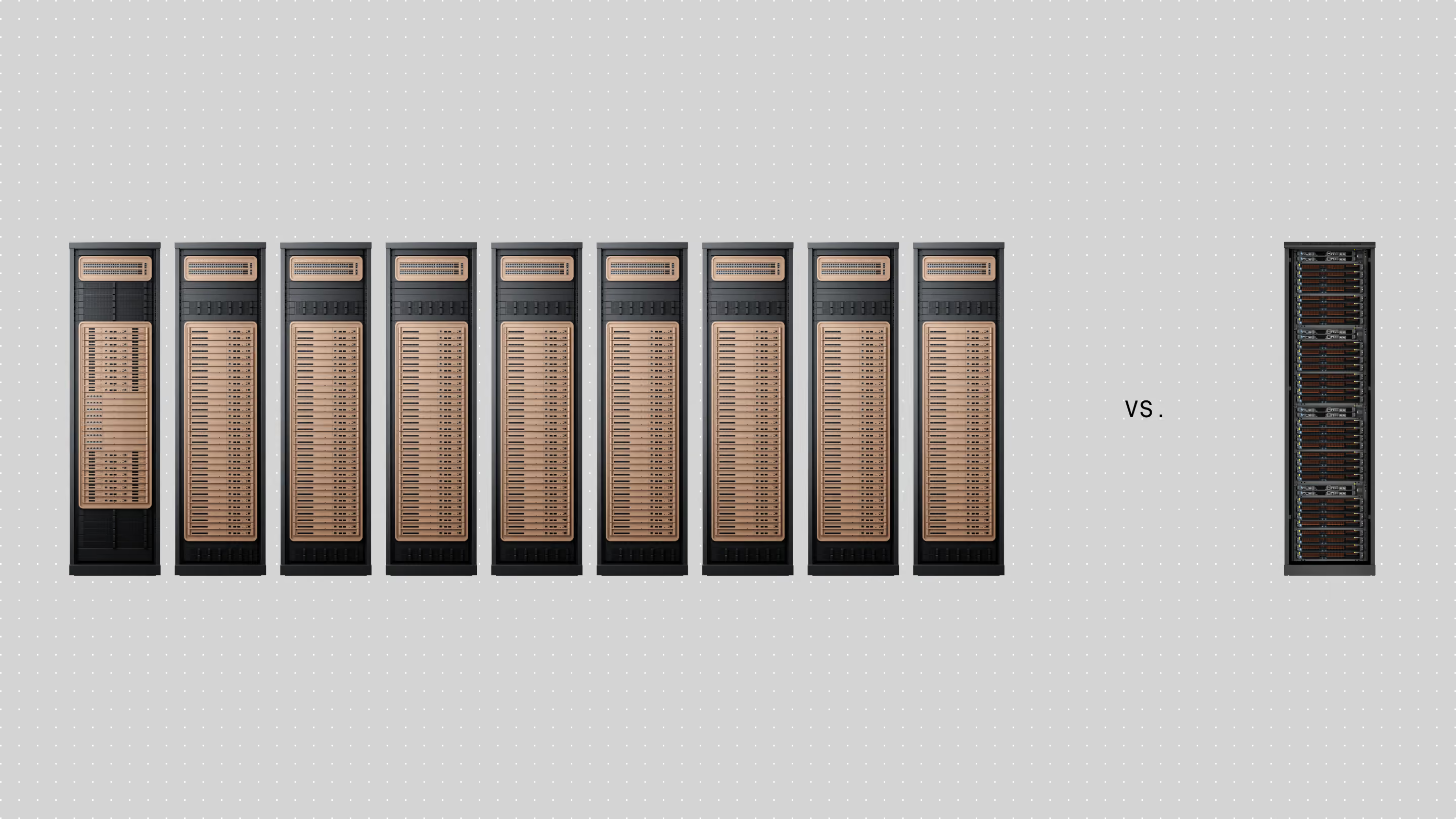
The results are giant multi-rack machines like the Nvidia+Groq combo introduced at Nvidia GTC 2026 with Jensen preparing users for a future in which one million tokens at 800 OTPS might cost up to 150 USD for a 2T parameter model 1 .
These are not good long-term solutions. They are workarounds – bolting together different systems to solve a problem neither architecture solves on its own. And they scale badly as model sizes increase toward 5T to 10T parameters.
What went wrong? Why do today’s systems fall short? Where do we go next?
No matter the solution, we know for sure that:
- Model sizes will increase driven by a competitive landscape in which multiple frontier labs are trying to outperform each other and where model size is still strongly correlated with model capability.
- Model speeds will have to increase because AI models are talking more and more directly to other AI models or APIs, instead of slower humans.
- Model costs will increase without a radically different approach from the current GPUs, TPUs, and LPUs.
We also face enormous challenges with energy consumption exploding as models get bigger and better. Many industry analysts believe that the increase in cost and power consumption are going to represent a global problem.
That’s why Tensordyne has been building from “the math-up” for our next generation of chips and systems for AI inference in datacenters. The result is that a single TDN Rack significantly outperforms nine Nvidia+Groq racks in speed, cost, and power – and delivers far better energy efficiency than other new stand-alone systems.
And now we get to tell you how we think about solving inference, what we did, how it works, and how it turned into a leap in system performance, density and efficiency.
Tensordyne Napier.
The Market Wants Fast, Cheap, and Smart
Model quality, response speed, and cost are no longer separate buying criteria. All three have to be solved together.
Let’s start with a quick take on the state of the AI inference market.
Everyone wants the biggest models
Modern AI models are large - and are getting even larger. Parameter counts have very quickly grown from DeepSeek-R1’s 671B parameters in early 2025 to Kimi K3’s 2.8T parameters in July 2026. There are 10T parameter models in training according to x.AI 4 with sources suggesting that Claude Mythos 5 is already running at 10T parameters 5.
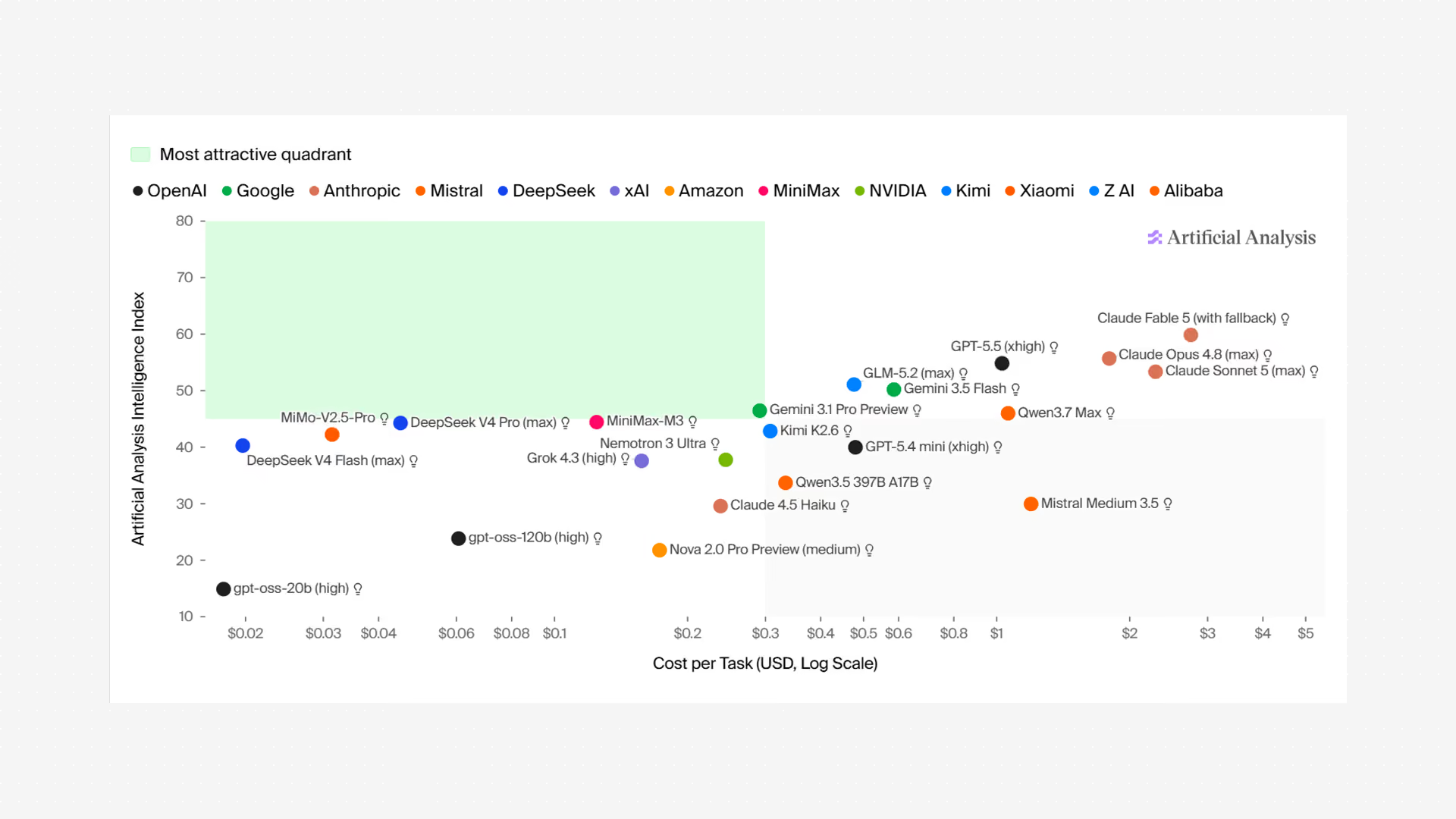
Many of today’s most popular and most powerful models are in the 1 to 3T parameters range and show a clear positive correlation between intelligence and price as shown in the chart above from ArtificialAnalysis.com.
Above all, users want speed
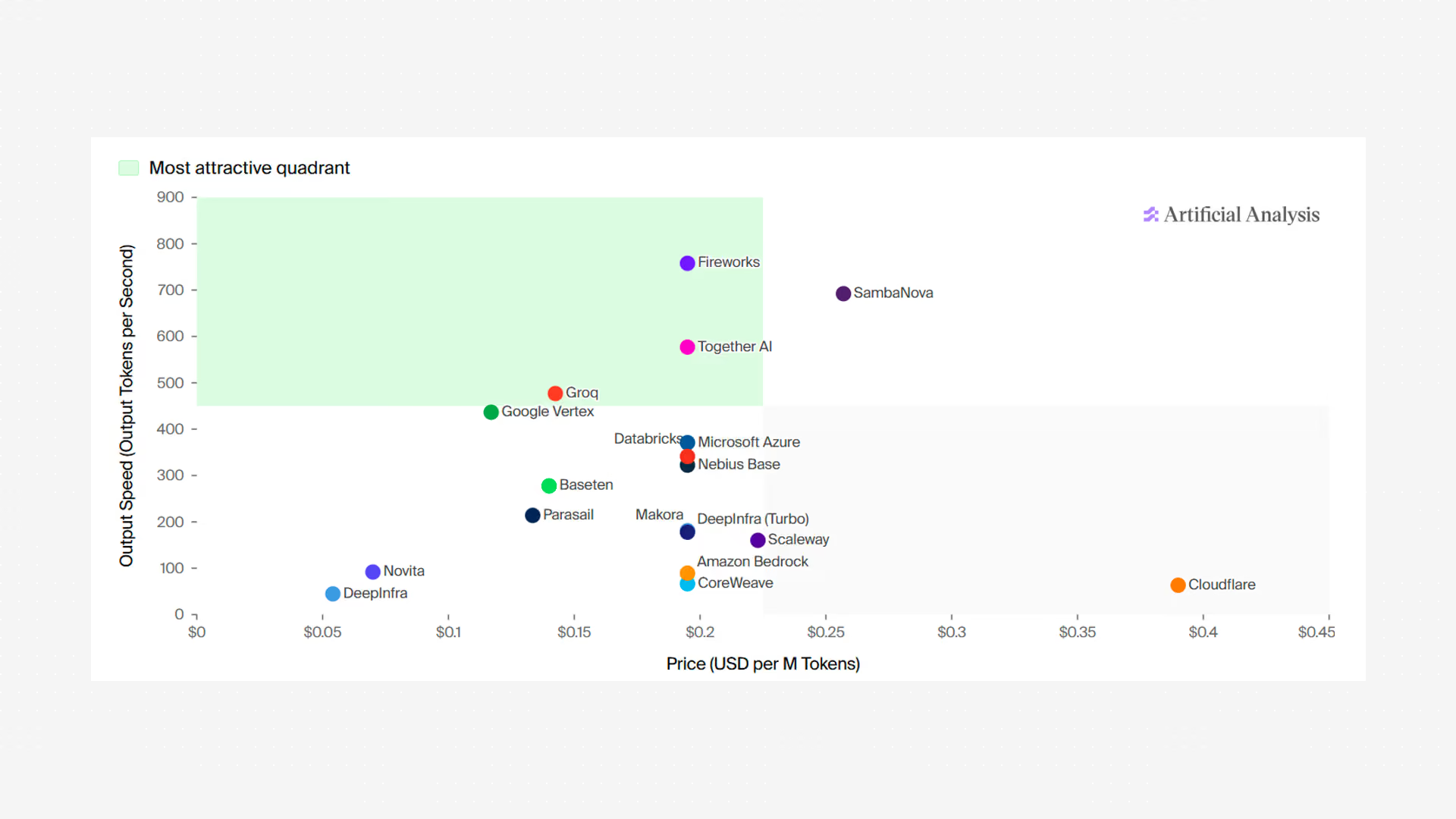
At the same time, people are willing to pay more for higher speeds as shown below.
But it must be affordable
People want better models, and they want faster models — and the data show they are very willing to pay more for it. The faster my tokens arrive, the more I am willing to pay for every one of those tokens. But there is a limit for what people can afford, otherwise it won’t help. Driving down the cost while driving up the speed for the biggest and best models matters.
Models. Speed. Cost.
What High-End Inference Requires
Peak compute is only one ingredient. Frontier models run at the speed of the bottleneck you neglected.
Amdahl’s Law states that a system is only as fast as its bottleneck. For a datacenter-level AI inference system, the main five are compute, memory bandwidth, memory capacity, fabric bandwidth, and fabric latency.
Compute: Enough math, in the right area and power envelope
Compute is what makes AI work. Wasted compute is wasted intelligence.
Inference has passed training as the bigger AI compute market in 2026 and along with that has come a shift in requirements. The focus for inference compute is to deliver better and faster models for the lowest possible cost and power.
AI is math at the fundamental level.
More cost and power efficient compute means using less silicon area and less power per math operation. Lower precision data formats help when the impact on accuracy is not an issue.
But it’s also about optimizing the sizes and shapes of matrix and vector compute based on model requirements and minimizing the energy and time spent moving data. Doing this well reduces idle time and increases utilization.
And very importantly compute must be optimized together with memory and interconnect.
Not enough compute limits what a chip can do. But too much compute with nothing to do because of insufficient memory or interconnect bandwidth is wasted investment.
Memory: Capacity and bandwidth must be designed together
Memory architecture can make or break model size, speed, and cost.
So how does this impact memory architecture?
A 10 trillion parameter model - assuming FP4 precision for parameters - requires 5 TB of fast memory just for the weights. That’s roughly a quarter of the 20TB+ of HBM (high-bandwidth memory) found in the largest systems from Nvidia and AMD that will start shipping later this year and into next.
However, when including KV cache (the users’ context) deploying a model like this might consume half or even all of a single rack’s memory to operate at sufficiently high speeds. One rack that costs on the order of ~$10M (5-year all-in TCO) to handle a single giant model.
But that’s only half of the story. Memory bandwidth is also crucial. The faster your memory bandwidth (TB/sec), the faster you will serve user output tokens. Simple as that. Compute is not what is bounding output generation. It is memory bandwidth. And on-chip SRAM has the highest memory bandwidth (even higher than HBM despite the name).
Most XPUs (AI accelerator processors such as GPUs or TPUs) today offer either relatively high amounts of on-chip “SRAM” memory (quite tiny in capacity, but fast in speed) or lots of external memory (HBM/DRAM) but little on-chip memory. This is because compute takes up so much space on silicon, that so far it has been very hard or even impossible to build XPUs that offer both HBM and large on-chip SRAM.
Why then is HBM the predominant memory used in systems that can run the largest models? Because it’s the best compromise between memory capacity (GBs) and memory bandwidth (TB/sec) per XPU. An SRAM-only system with 0.5 GB per chip would require an astounding 10,000 chips just for the model weights of a 10T parameter model – clearly uneconomical.
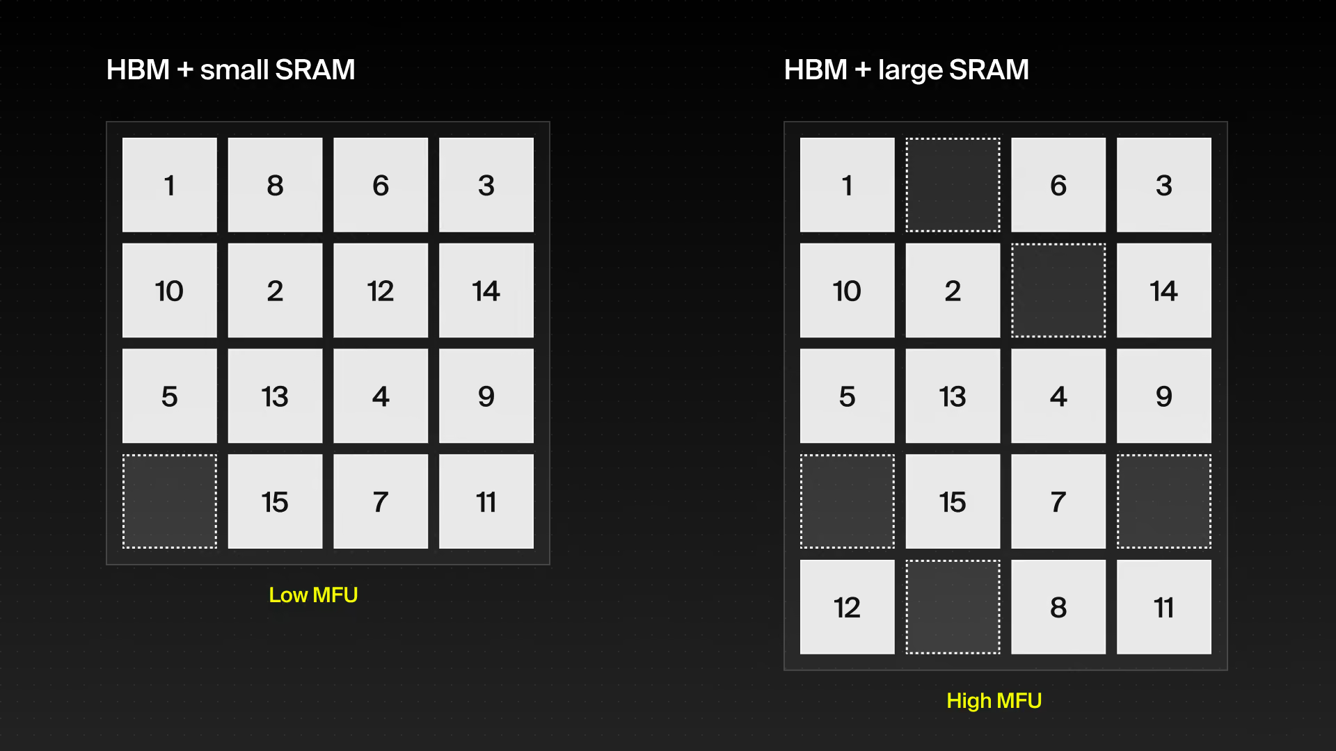
But on-chip SRAM memory is still extremely essential to achieve high system utilization and performance (and thereby low cost) for systems using HBM or DRAM to solve the capacity problem. SRAM acts like a buffer that the Compiler (the software that orchestrates the execution of all these complex AI model workloads) and the CPUs get to work with.
It works a bit like a Sliding Puzzle game where the size of the puzzle represents the size of the HBM/DRAM and the empty slots represent the size of the SRAM. Pairing a large HBM with a small SRAM results in few empty spaces and the Compiler struggles to get the highest MFU (Model FLOPS Utilization) from the system.
But lots of SRAM in an XPU translates to more empty slots, which gives the compiler more room to work and makes workload orchestration easier (e.g. fusing operators and doing them “in one go” instead of buffering in HBM after every small operation) resulting in much higher MFU.
Interconnect: Bandwidth matters, but latency often sets the ceiling
Serving the best models puts extreme pressure on interconnect. Get it wrong and user speed takes the hit.
Chip-to-chip communication – or rather XPU-to-XPU communication – has become such an important cornerstone of AI compute that companies like Nvidia have literally started putting their respective technology’s name into their product names themselves. ‘NVL72’ is Nvidia’s flagship product (both Blackwell and Rubin generations) where NVL stands for NVLink – their in-house “scale-up fabric” that provides the interconnect for communication between chips.
The biggest driver behind the increasing importance of scale-up fabric has been and will be MoEs (Mixture of Experts), an AI model architecture which lends itself perfectly to parallelization over as many as 100+ XPUs.
That being said: There is not a single AI model architecture that does not benefit greatly from fast chip-to-chip connectivity which supports all forms of parallelism.
A scale-up fabric (as the term ‘fabric’ suggests) is essentially a mesh (=fabric) of high-speed point-to-point communication links, connecting every chip/XPU to every other chip/XPU in a system through a direct point-to-point connection (hence “any-to-any” or “all-to-all”).
In other words: every XPU within a system can ‘talk’ directly to every other XPU. This means that every one of the 72 GPUs in an NVL72 has a direct NVLink connection to each of the other 71 GPUs.
This form of any-to-any connectivity is essential in AI inference for two reasons.
First, even with HBM a single device can never have enough memory capacity to deploy large modern AI models all by itself - large models such as DeepSeek R1 with close to 700 billion parameters require at least 350 GB in FP4 precision without taking KV cache (users’ context) into account. Hence a minimum of 4, 8, 16 or more XPUs are necessary to map large AI models which are growing in size as discussed above.
Second, even for models that would fit into the memory of a single XPU, the only way today to scale users’ speeds at which the AI model is executed/served to them beyond that single chip’s ability is to spread the work (“parallelize”) among multiple XPUs.
The whole point of a scale-up interconnect is to minimize the time it takes to move data between chips to maximize user output token generation speeds. Here we need to discuss the importance of latency vs bandwidth. When transferring large amounts of data, the bandwidth is most important. But in large MoEs deployments with wide Expert Parallelism, chip-to-chip communication is usually as short as a few Kilobytes which are transferred on a nanosecond scale. Hence bandwidth becomes irrelevant and the latency one has to “pay” as a ground floor of communication cost is much more relevant than the bandwidth for maximizing user speed.
Parallelism: When one chip isn’t enough
Parallelism brings together multiple XPUs to make an AI model go faster, go cheaper, or go bigger.
Tensor Parallelism (TP)
In “TP”, a single large mathematical operation such as a large matrix multiply gets executed on multiple XPUs in parallel. Think: every XPU does only a portion of all the result-matrix’s columns. The partial results have to be shared between them through the scale-up fabric.
How it works: XPU n is performing slice n of a MatMul operation, XPU n+1 is performing slice n+1 of that same MatMul operation.
Requires any-to-any fabric? Yes!
Speeds up per-user speed? Yes!
Tensor parallelism is great for making large operations go faster. But the wider the TP, the more pressure it puts on the interconnect.
Pipeline Parallelism (PP)
With pipeline parallelism, multiple XPUs are connected in series instead of acting “next to each other” like in “TP”.
How it works: XPU n completes an operation and passes the baton to XPU n+1 to perform the next operation.
Requires any-to-any fabric? No, sequential
Speeds up per-user speed? No.
The term ‘parallelism’ is almost misleading here. Yes, multiple XPUs are acting in parallel time-wise, but they are serving different active users because of the auto-regressive and sequential nature of AI models.
The big down-side compared to TP: the parameters of a model are indeed split over multiple XPUs because each XPU processes a subgroup of all layers, but the KV cache (user context) is as large per XPU as it would be without any parallelism due to the auto-regressive loops in LLMs (Large Language Models).
For SRAM-only XPUs, Pipeline Parallelism is often used to split model weights across hundreds to even thousands of chips because each XPU’s on-chip memory bandwidth is very fast but capacity is very low.
Expert Parallelism (EP)
This form of parallelism was born with MoE (Mixture of Experts) models which, unlike ‘dense LLMs’, are rather sparse compute graphs in the sense that out of the large pool of model parameters grouped into so-called “Experts”, only a fraction of them are actually activated. DeepSeek-R1 for example, has 58 expert layers with 256 experts each, but only 8 experts are loaded per layer.
How it works: Each XPU has only a subset of experts, e.g. for DeepSeek-R1 with 256 experts per layer and 64 XPUs, only 4 per layer are put on each XPU.
Requires any-to-any fabric? Yes!
Speeds up per-user speed? Yes!
Depending on the number of parallelly served users, this can massively reduce the amount of “active experts per node” for each token generation, and hence reduce the amount of Gigabytes that need to be loaded from HBM/DRAM into the XPU’s on-chip memory for processing. The result is reduced time to load experts and increased user speeds.
On the other hand, if a very high number of users are active per XPU, then all the weights are loaded on every node since there it is likely there is at least one user requiring any expert to be loaded. But even in this case EP is highly beneficial.
Note: Expert and Tensor Parallelism are often combined in MoE inference - for different parts of the graph – as it usually also has a ‘dense’ portion and not just the ‘sparse’ routed experts.
Data Parallelism (DP)
Data parallelism is a way to process more users by running identical copies of an AI model.
How it works: Find the best TP for the model and use Data Parallelism to run as many copies as possible. If TP=8 works best and you have 64 XPUs, you can run 8 instances (DP=8): 8 * 8 = 64 XPUs.
Requires any-to-any fabric? Depends
Speeds up per-user speed? It can
For MoE, it can also be used to separately optimize performance of different types of layers. For example, EP64 may be optimal for expert layers, but high TP may introduce inefficiency. By using TP16+DP4 for attention layers and EP64 for expert layers, you can keep 64 chips busy and minimize overall latency.
Sequence Parallelism (SP)
Parallelism can also work on the dimension of the input sequence. This is typically used for Prefill, where all the input tokens are known ahead of compute time and can be split across multiple XPUs. Decode is different: output tokens have to be generated one after another.
How it works: One XPU processes the first 1024 tokens of a long input sequence, the next XPU handles the next 1024 tokens in parallel, and so on.
Requires any-to-any fabric? No
Speeds up per-user speed? Yes!
Sequence Parallelism is great for speeding up long Prefills. But it doesn’t help with sequential Decode.
Context Parallelism (CP)
Context Parallelism splits a user’s context and KV cache across multiple XPUs. It becomes increasingly useful as context windows grow to hundreds of thousands or even millions of tokens and the KV cache becomes too large or too slow for one XPU to handle efficiently.
How it works: Each XPU stores and processes a portion of the context. During attention, they work on their portions in parallel and combine the results.
Requires any-to-any fabric? Helps
Speeds up per-user speed? Yes!
Unlike Sequence Parallelism, which is primarily used during Prefill, Context Parallelism can also help during Decode because every new token still needs to attend across the existing context.
User Parallelism (Batch Size/ Continuous Batching)
While it is usually not referred to with this name, it is important to also mention the parallelism of multiple users in actual deployments which includes time-wise randomness and non-uniformity.
Batch parallelism refers to processing multiple users in groups (batches) to increase compute utilization and drive down costs.
Continuous batching is an often-used umbrella term for approaches describing how to handle multiple users’ randomly incoming input and output processing (prefill and decode) demands.
How it works: An XPU handles multiple user requests at one time, allowing a group of weights to be loaded and used multiple times. Chunks of prefill and decode can also be overlapped and intermixed.
Requires any-to-any fabric? No
Speeds up per-user speed? It can.
User parallelism is an important way to increase compute utilization and drive down costs.
Parallelism Summary
Technique
Primary purpose
Any-to-any fabric?
Increase user-speed?
Tensor Parallelism
Splits a large operator across XPUs to increase per-user speed.
Yes
Yes
Pipeline Parallelism
Places model stages in sequence; useful for capacity and throughput.
No
No
Expert Parallelism
Distributes MoE experts across XPUs; can sharply reduce active weights per node.
Yes
Yes
Data Parallelism
Runs parallel instances of models or layers within a model to increase throughput.
Depends
Depends
Sequence Parallelism
Splits known input sequence work across XPUs during prefill to increase per-user speed.
No
Yes
Context Parallelism
Splits KV cache across XPUs to increase per-user speed; useful for capacity.
Helps
Yes
User Parallelism
Combines irregular user work to improve utilization.
No
Depends
Which brings us to the question, “is disaggregation another form of Parallelism?” Absolutely! But it demands its own section below.
Disaggregation: Leading the pack or playing catch up
Prefill and decode stress the system differently. Disaggregation lets you optimize the hardware for each phase, but the handoff can become the bottleneck.
Everyone is talking about disaggregation these days, but what is it?
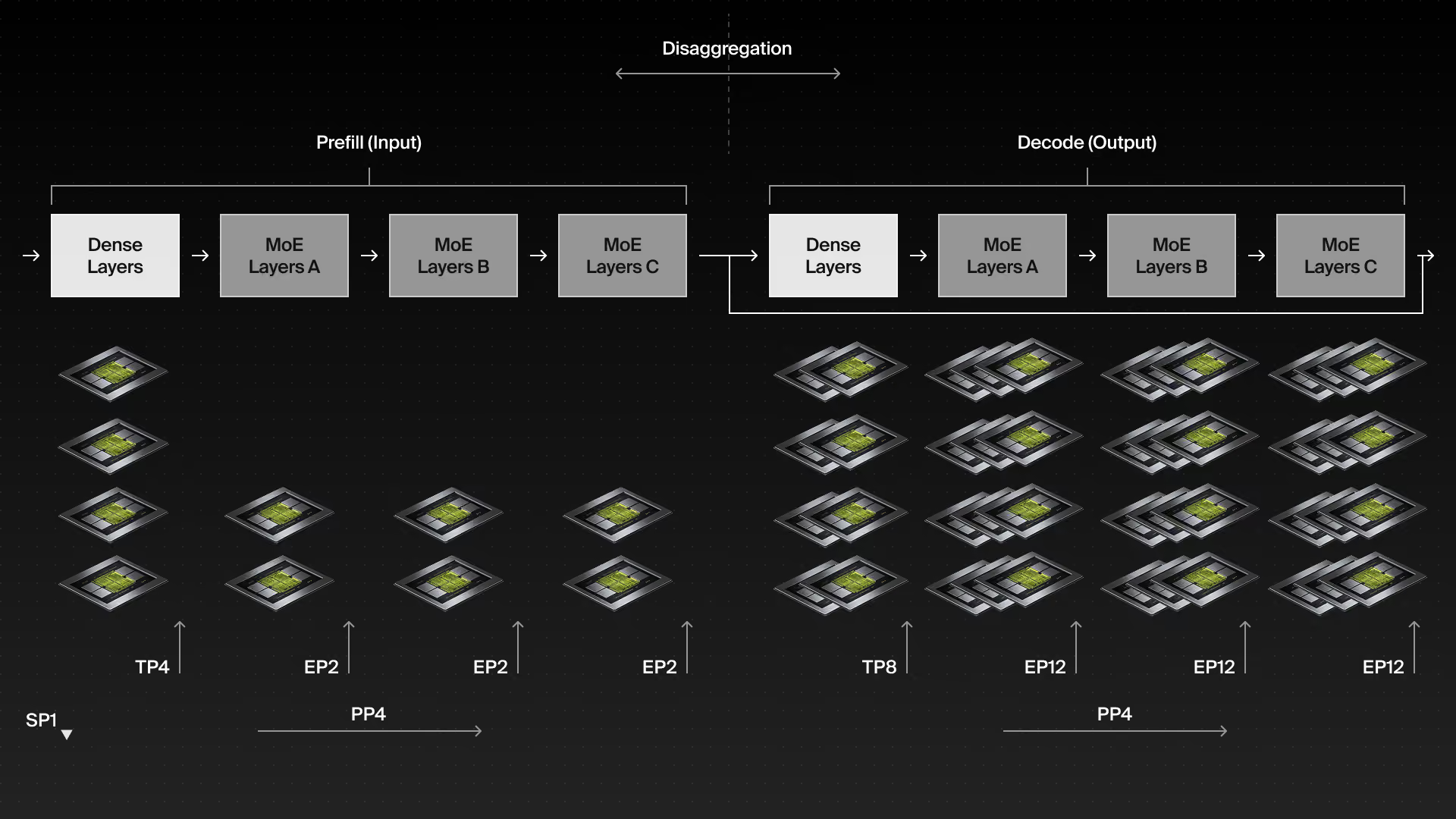
Disaggregation is a form of ‘phase parallelism’ – although most people don’t call it that – that is essential to getting the most out of systems in terms of per-user-speed. It went viral following Nvidia’s Groq deal and is on track to becoming a staple for large-scale, high-speed inference in datacenters.
The core idea: Prefill usually outperforms decode in token generation speed (total tokens per second across all users) due to the difference in phases: prefill is compute-bound whereas decode is memory-bandwidth bound. Hence it would make sense to allocate a few chips to Prefill, and a lot more chips to Decode. This creates better balance. And effectively brings down cost and increases per-user-speed.
In addition, since some XPUs have much higher compute while others have much higher memory bandwidth, it’s not surprising that some companies are - as mentioned above - taking it now to the next level to combine multiple types of systems.
By now there are three distinct forms of disaggregation:
Disaggregation A: Same chip, optimized by task
Same XPUs (homogeneous) using the same memory approach.
Config: XPU-A: n chips for Prefill, m chips for Decode.
This approach only helps if that one XPU can scale very nicely to a high degree of TP/EP without hitting bottlenecks. Basically, if for your given workload your XPU can cover both phases.
Here it’s all about throughput balancing of Prefill vs Decode to achieve high per-user-speed at low cost.
Disaggregation B: Same chip, optimized by memory
Same XPUs (homogeneous) using different memory approaches.
Config: XPU-A: n chips for Prefill using HBM, m chips for Decode using SRAM
Very few systems can do this as most won’t have both HBM and a lot of SRAM per XPU.
Here it is about achieving the highest per-user-speed possible.
Disaggregation C: Two chips, constrained by memory
Different XPUs (heterogeneous) using different memory approaches.
Config: XPU-A: n chips for Prefill using HBM, XPU-B: m chips for Decode using SRAM
Here it is about combining two systems to overcome each other’s shortcomings and extend the overall performance.
This is the Nvidia+Groq, AWS+Cerebras, and AMD+Cerebras approach. Two entirely different systems connected through non-fabric high-speed ethernet. Very expensive, high power, and limited per-user-speed due to rack-to-rack latency.
The Disaggregation Challenge: The common thread
All disaggregation concepts have a common challenge:
If the interconnectivity between the Prefill- and the Decode-groups of XPUs is a bottleneck, the approach does not scale well. Both intra- and inter-group interconnectivity need to have high bandwidth (>1TB/sec) and even lower latency (2us and lower) to achieve highest per-user-speeds and lowest cost.
Tensordyne: Napier at a Glance
We changed the arithmetic itself, then rebuilt everything above it to match. The number format, the chip, the trays, the interconnect.
Before we take a look at how others stack up, let’s take a quick look at Tensordyne Napier.
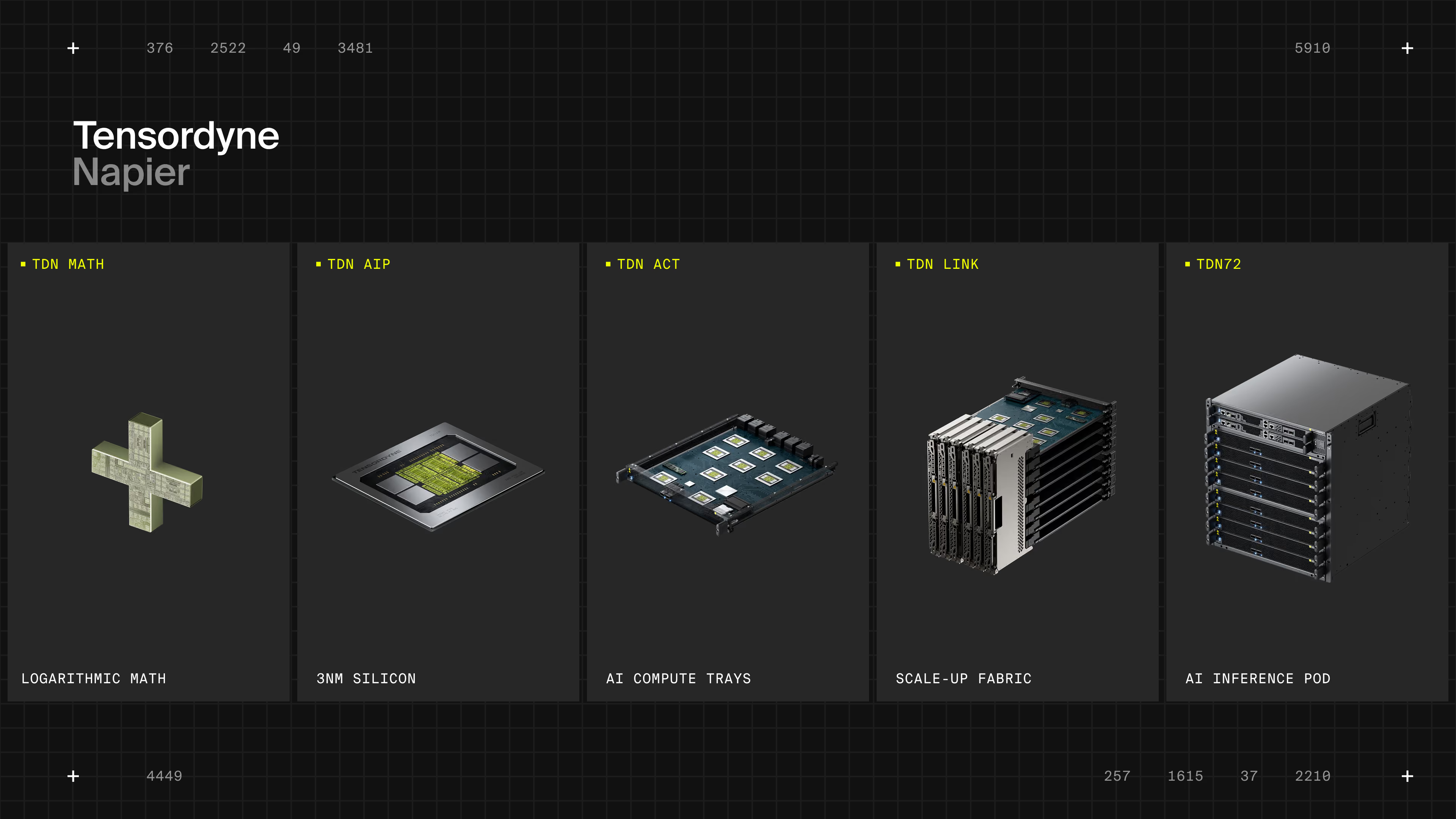
Introducing the Tensordyne Napier (TDN) generation system, designed specifically for the needs of AI inference.
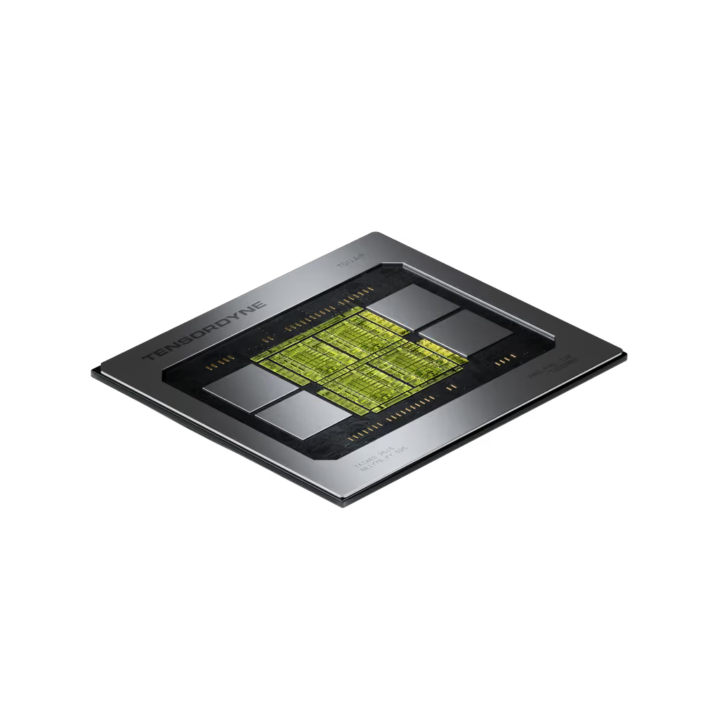
It starts with our logarithmic math. TDN Math significantly reduces compute area and power, enabling a fundamentally better allocation of silicon. We bring together an optimized combination of compute, SRAM, HBM3e, and our TDN Link ultra-low latency interconnect in our TDN AIP (Artificial Intelligence Processor). Built on TSMC 3nm, it is the most efficient AI inference chip for datacenters.
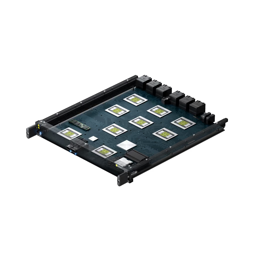
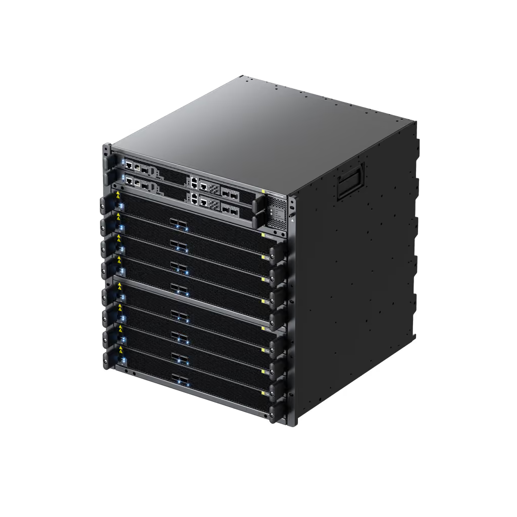
Multiple AIPs sit on each AI Compute Tray (ACT) which also have an Intel CPU, storage, and scale-out networking. Compute trays are brought together with TDN Link fabric in our TDN72 pod, providing a total of 72 chips with any-to-any connection to support all forms of parallelism and disaggregation.
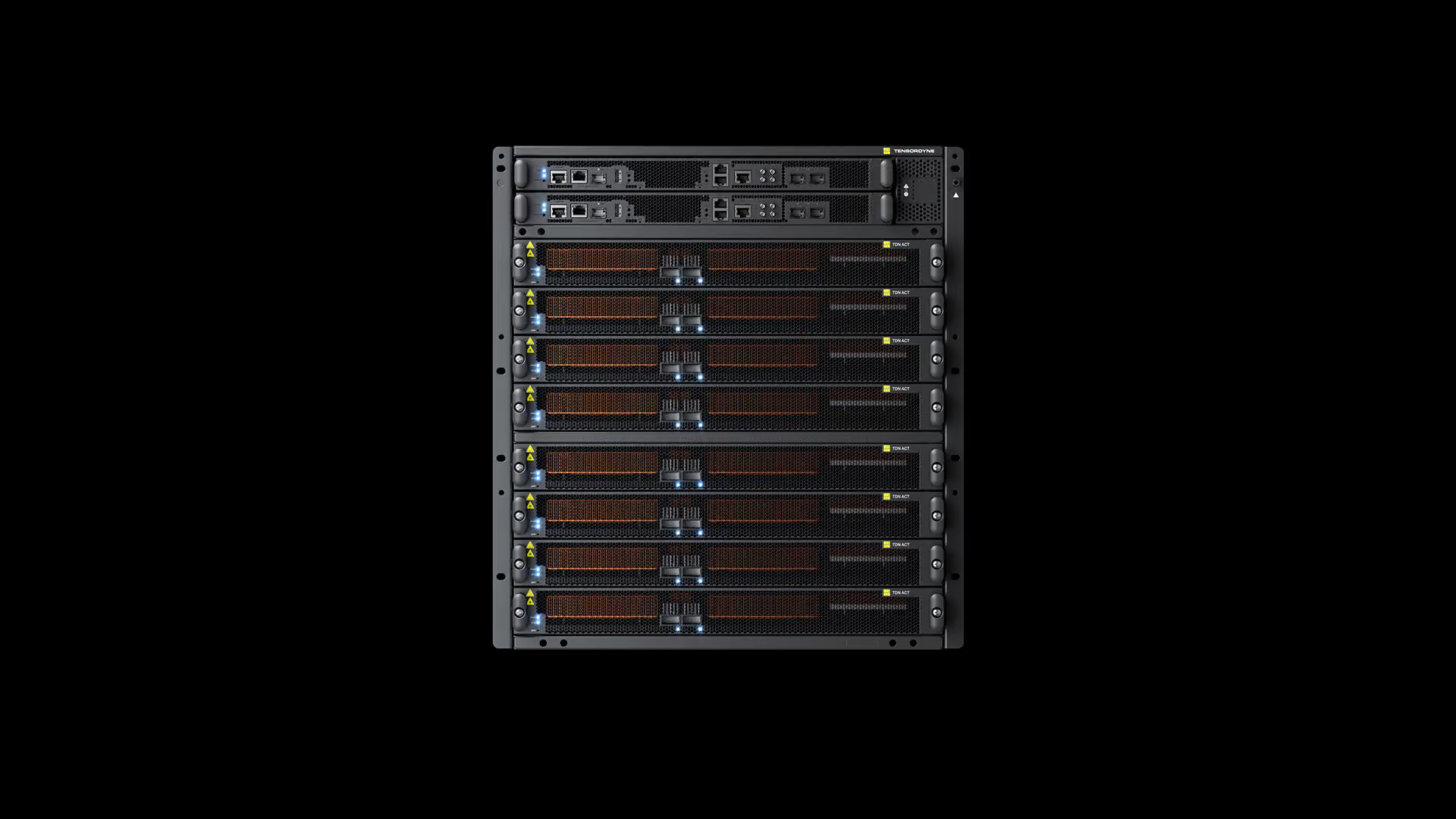
TDN72 Pod
System
TDN72 (Napier Gen)
Configuration
72x Tensordyne TDN AI Processors
AI Compute FP8 a
151.9 PFLOPS
AI Compute FP16 a
76.7 PFLOPS
HBM Capacity
10.4 TB @ 338 TB/s
Scale Up Bandwidth b
68.8 TB/s
Frontend IO Ethernet
8x dual-200-Gbps QSFP Ethernet
x86 cores
8x 10-core Intel Xeon D
Storage
64 TB
Physical Dimension
13RU (44.2 x 57.8 x 81.3 cm)
System Cooling
Air Cooled (Rear Fan Trays)
Operating Power
30 kW
HVAC (180-305 VAC) 15A / 20A
HVDC (190-410 VDC) 15A / 20A
a dense (no sparsity)
b total bidirectional system bandwidth (72 any-to-any direct connectivity)
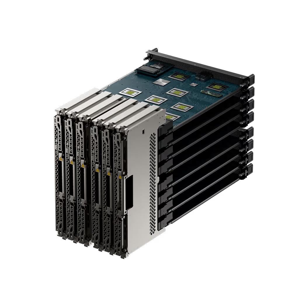
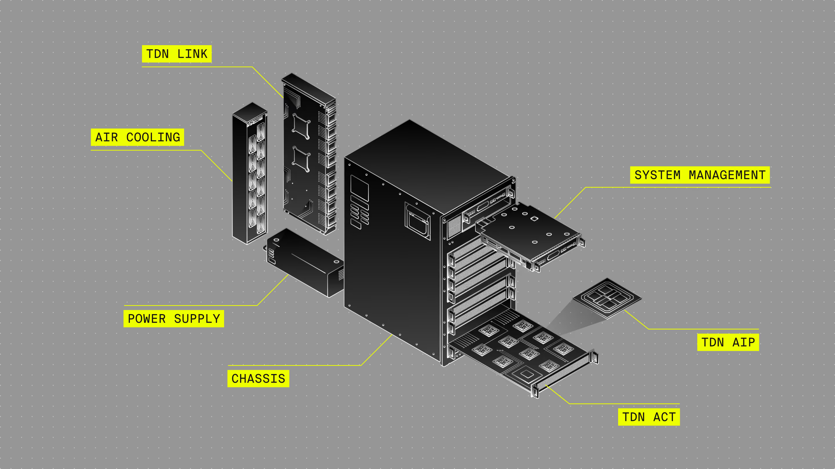
The TDN72 combines TDN ACTs with industry-proven management cards, power supplies, air-cooling, and chassis and serves as the core-building block for a disaggregation-enabled AI inference factory:
- Eight TDN ACTs (AI Compute Trays)
- Six TDN Link scale-up fabric cards
- Two management cards
- Redundant power supplies
- Air-cooling fans
- 13 RU (Rack Unit) chassis
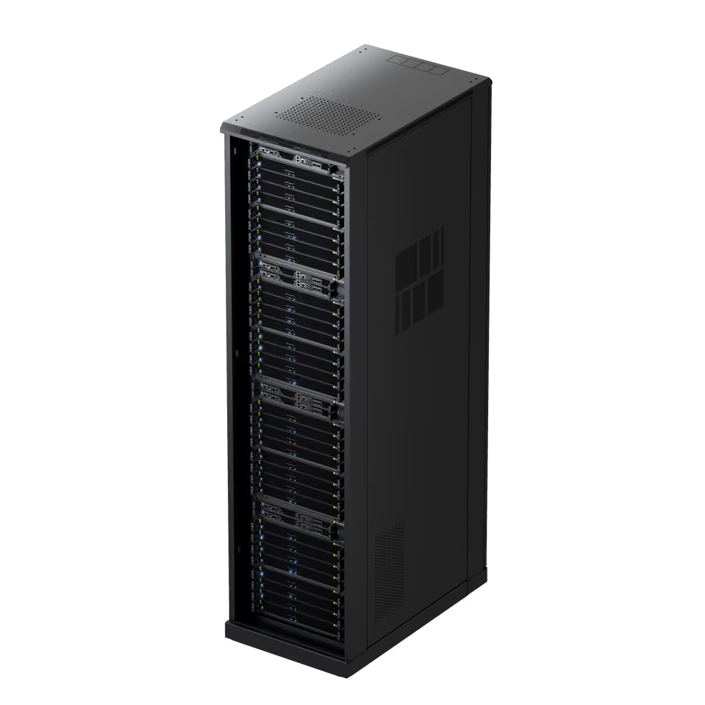
Four TDN72 pods can fit in a standard 52RU datacenter rack to support the largest models at the fastest user speeds:
- 608 PFLOPS of FP8 dense compute
- 72 GB of SRAM
- 41.5 TB of HBM3e memory
- 275 TB/s of any-to-any interconnect with <1.5 µs latency
- All for less than 120 kW
Our TDN72 with SRAM+HBM and any-to-any connectivity is topologically similar to Nvidia NVL72 and AMD Helios. This significantly reduces the migration cost to “port” or migrate a model deployment that was tuned for the Nvidia or AMD racks (both with 72 GPUs) over to Tensordyne as future datacenters shift more and more to multi-vendor implementation.
TDN Link (Scale-Up Fabric)
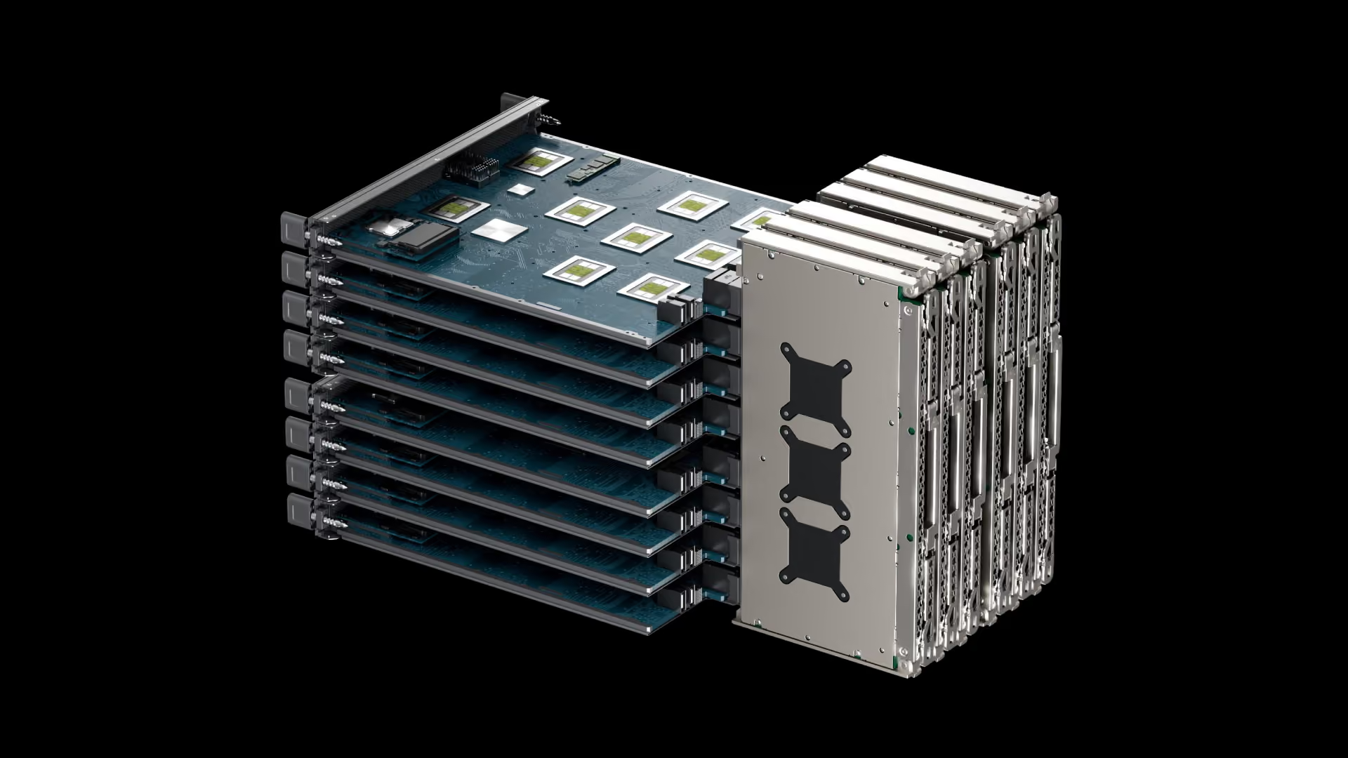
Six TDN Link fabric cards provide high-speed any-to-any connections between 72 chips and are mounted at the back of the chassis orthogonal to the 8 compute trays.
- Six TDN Link scale-up fabric cards
- 11.5 TB/s scale-up bandwidth per card
- < 1.5 µs latency
- Impedance-matched copper traces ensure matched timing between chips
- 99.999% proven up-time with fault-tolerance in HPE Juniper systems 6
TDN ACT (AI Compute Tray)
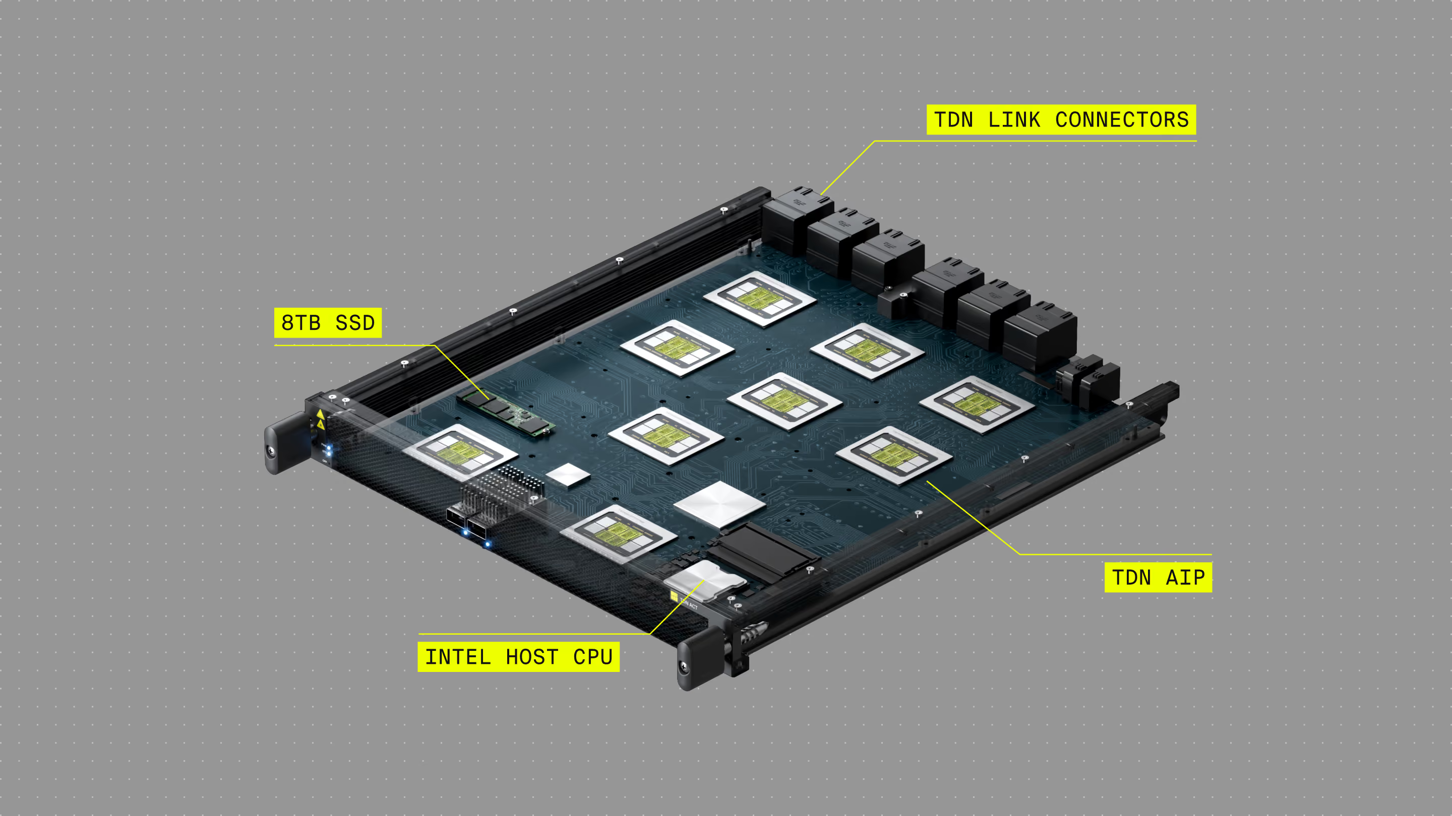
Our TDN ACT is the densest compute tray design ever, packing nine AIPs in a height of just 1 RU (Rack Unit):
- Nine TDN AIPs (AI Processors) for a total of 19 PFLOPS (FP8 dense) compute
- 1.3 TB of HBM3E at 42 TB/s total bandwidth
- 8TB of NVMe SSD (e.g. for local model storage or local KV cache pages)
- Intel Xeon-D processor (running our TDN Inference Server)
- Six TDN Link connectors at the back for scale-up
- Dual 200 Gbps Ethernet optical links at the front for scale-out
TDN AIP (AI Processor)
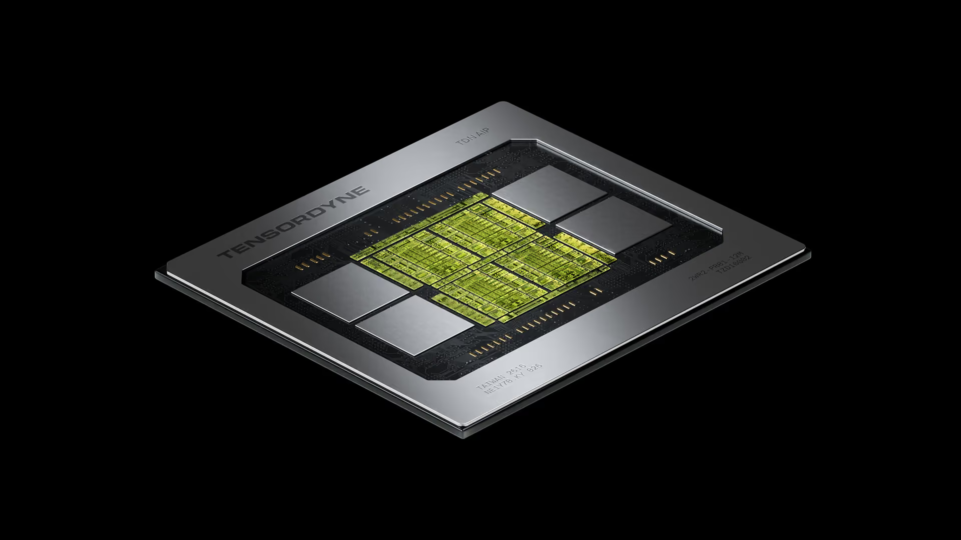
MCM
TDN AIP (Napier Gen) in 3nm TSMC
AI Compute FP8 a
2.11 PFLOPS
AI Compute FP16 a
1.07 PFLOPS
Vector Processing
Dedicated VPUs
Supported Precisions b,c
FP16, FP8, FP4, NVFP4
On-Chip SRAM Memory
256 MB @ 40 TB/s
HBM3E Capacity
144 GB
HBM3E Bandwidth
4.7 TB/s
Scale Up Fabric Latency
~ 1000 ns
Scale Up Fabric Bandwidth
1.0 TB/s
Host Connectivity
PCIe Gen5 x8
TDP
300 W
a dense (no sparsity)
b Dynamic scaling for all datatypes
c FP4 and NVFP4 supported only for parameters/weights
The TDN AIP (AI Processor) with TDN Math is the world’s first logarithmic math chip for AI inference:
- 2.11 PFLOPS of FP8 dense compute
- 256 MB of SRAM
- 144 GB of HBM3E
- 1.0 TB/s of scale-up any-to-any interconnect
A new class of inference system
Rather than combine separate HBM-centric and SRAM-centric systems, Tensordyne Napier combines the best of all – efficient compute, high-capacity HBM, unusually large on-chip SRAM, and low-latency scale-up connectivity – in a single system.
The AI Inference Landscape: Every Architecture Is a Bet
The market contains many innovative approaches, each optimized around a different constraint and betting on a certain future. But the ChatGPT moment changed the rules, putting new stress on those designs. Looking at the different bets shows where Napier is different.
Now that we know what is needed, we will answer the questions: What went wrong? Why do today’s systems fall short?
There’s no denying that today’s systems include many remarkable innovations, like Cerebras’s wafer-scale chip or Groq’s SRAM based LPUs. Even so, many of the limitations are due to architectural decisions that were made prior to the ChatGPT moment. Or were impacted by specific workload demands. Like fast SRAM-only systems developed for “smaller” models or GPU systems that also must support large-scale training and not just inference.
To understand why both the giants and startups are hitting a wall, we will divide the chip company landscape into fairly distinct camps to look at the trade-offs they have made. Let’s start by introducing the groups and provide some examples of each:
The Bakers
(Taalas, Etched, Lamb labs)
They bake functionality or models into silicon. Very fast. But at the cost of architectural flexibility.
The On-Chippers
(Cerebras, Groq, Fractile)
Fast output generation. But expensive to scale for today’s large models.
The Budgeteers
(D-Matrix, Positron, Tenstorrent, Rebellions, Furiosa)
Designed for lower cost. But not to push the frontier of model scale at high user speed.
The Versatiles
(Nvidia, AMD, Intel, Hyperscalers)
The big guys. Lots of HBM, compute, and scale-up. Flexible enough to run almost anything, but not optimized for the highest per-user speeds.
The Tokenmaxxers
(Tensordyne)
Large SRAM and HBM. Fast, wide, low-latency scale-up. Optimized for more tokens, faster tokens, and less power.
The Bakers: Models burned into silicon. Locked in for life.
Companies such as Taalas and Etched pursue efficiency by specializing silicon around a model or a constrained set of functions.
Companies like Taalas and Etched are quite public about baking fixed models or functionality into silicon. Taalas goes to the extreme and bakes just a single model into a chip. Is it fast and cheap? Yes, but every model requires a new silicon spin. It takes months to years to react to a new model release/ architecture. Plus, this approach is very limited in how large (and thereby: how good) the models are that can be mapped to this approach (memory-constrained).
Etched is a company that follows this approach even if slightly less extreme, by baking certain often-used functions into silicon (thereby enabling e.g. their “Low-Voltage Inference”) although they do use off-chip memory to store weights. “We are taking a huge bet”, states their CEO.
The problem with baking fixed functions into silicon is history: In the last many years the biggest leaps in AI capability have always originated from new AI model architectures. Hence betting on its consistency is fragile by concept.
In other words: Frontier labs like Anthropic, OpenAI, Thinking Machines and Mistral don’t like the idea of being bound to one kind of model architecture - they simply do not know how significantly their models will change in six months from today.
The lack of architectural flexibility is what The Bakers have in common.
The On-Chippers: Fast. As long as it fits.
Groq, Cerebras, and others bet on massive on-die memory bandwidth feeding deterministic execution. High per-user speed as long as the model fits in a memory measured in megabytes, not terabytes.
Interestingly this is the space that recently has been landing the highest valuations. Groq “sold” – or rather licensed/was acqui-hired – for $20B to Nvidia 7. Cerebras has landed deals with hyperscalers on their path to a remarkable $50B+ IPO 8.
But what many don’t know is that both of these companies developed their approach many years before the “ChatGPT moment”. Their designs were developed for much smaller models from the AI vision era, like object detectors with 100M parameters, and not for the 1T parameter models being run today which are literally 10,000x larger.
“Small” memory was fine back then but supporting even small to mid-size models like Llama 3.3-70B requires multiple racks worth of chips (4 for Cerebras and 9 for Groq) to have enough SRAM for the model alone.
The idea behind this approach today is simple: By using on-chip SRAM memory (as opposed to higher-capacity DRAM or HBM) they have very high memory-bandwidth for tasks that are bound by memory-bandwidth like decode, i.e. output token generation in LLMs (not so much for prefill).
The good is that major large-scale AI inference applications such as Co-Pilot coding, customer/sales automation, trading, analyst work and many others show a very strong correlation between higher per-user speed, and users’ willingness to pay for AI. For companies that provide TaaS (Tokens as a Service) in the current cut-throat market that’s driving margins to the bottom, offering significantly higher per-user speed is a way to (re)capture a market share in higher-margin segments.
Essentially: The faster the system can serve a single user, the more people will pay for each token. This linear correlation can be observed on platforms such as artificialanalysis.ai and other similar price/speed AI-API comparison platforms.
But the bad is memory capacity. On-chip memory (SRAM) rarely exceeds 0.5 GigaBytes per chip and requires hundreds to thousands of chips for state-of-the-art models like those from DeepSeek. This means high CapEx costs and large datacenter footprint just to run a single model. And models are growing: Kimi K3 is now already at ~3T parameters, ~4x the size of DeepSeek-R1.
Hyperscalers understand: On-Chipper systems cannot operate economically as standalone systems. They need to be paired with the systems they are building themselves. More on that later.
The Budgeteers: Play it safe. The money is in the middle.
Modular XPUs, cheaper memory, aggressive cost points. This group targets the enormous mass of workloads that don't need frontier hardware, only frontier economics.
The Budgeteers are trying to match what the big guys are doing, but at lower cost and smaller scale. They rarely go for full rack-scale solutions but use smaller, more modular form factors such as PCIe cards or OCP OAM modules. This limits the benefit of tensor parallelism as PCIe is more of a high-speed point to point interconnect and was never intended to be a scale-up fabric. They do use off-chip memory to meet the capacity needs of large AI models, but many stay away from expensive HBM and use slower and more affordable DRAM. The result is a system that competes in the lower-budget TaaS (token-as-a-service) segments of the market. Although they can scale to a large number of chips, they are mostly missing state-of-the-art scale-up interconnect.
All-in-all a reasonable approach for cost-sensitive inference, but not one designed to push the frontier of model scale and per-user speed.
The Versatiles: Build for many users. At the expense of every user.
Nvidia, AMD, Intel, and hyperscaler-designed XPUs combine substantial compute, HBM, mature software, and large scale-up domains and deliver high total throughput rather than high-user speeds.
The Versatiles can be split into two sub-camps:
- Nvidia, AMD and Intel as the neutral/ third party players
- Hyperscaler and model builders who are building their own in-house chip. Companies like OpenAI, Microsoft, x.AI, Meta, AWS, Google, etc.
What they have in common is that they all build a similar kind of system. Differentiation is decreasing, not increasing. Many in-house solutions aim to reduce Nvidia dependence and optimize for specific internal workloads rather than maximum performance across the board.
The recipe: Lots of FLOPS (Floating Point Operations Per Second) per chip. Single-hop inter-connect through any-to-any scale-up (e.g. Nvidia NVLink or Broadcom Tomahawk). Paired with fast HBM memory. And squeezed into a datacenter rack with liquid cooling to fight the high-density heat dissipation. 100kW to 250kW (and very soon 600kW) per rack.
But how many of those FLOPS do useful work? We calculate that Blackwell Ultra achieves a little over 10% MFU (Model FLOPS Utilization) during compute-bound prefill on DeepSeek-R1 based on SemiAnalysis InferenceX results as of August 2026 9. Early Rubin results from CoreWeave 10 put it at ~2% for the same model. Even during the compute-bound phase, the vast majority of theoretical FLOPS are left on the table.
These systems achieve the biggest spread and flexibility between speed and efficiency. A range of them can even be used for AI training as well. They are the best compromise of all.
But they lack the ability to run AI inference as fast as the Bakers and the On-Chippers.
This is the reason why the Versatiles have started building hybrid setups in combination with the On-Chippers: Nvidia+Groq, AWS+Cerebras, AMD+Cerebras, etc. As SemiAnalysis recently put it: “Nvidia wanted the IP (Groq) not to replace GPUs, but to extend them.”
It’s a way to address the speed limitation. But it comes with another system, another network boundary, and substantially more cost and power.
The Tokenmaxxers: More tokens. Faster tokens. Less power.
Tensordyne’s AI inference bet is that building from the math up matters. Change the math, and you change the trade-offs everywhere above it. It’s not about winning on FLOPS, SRAM, HBM, or interconnect individually. It’s about how much the whole system can deliver for every watt.
A “Tokenmaxxer” is a person who tries to use more tokens than anyone else. From an AI inference perspective, a Tokenmaxxer system is one that generates more useful tokens — running the biggest and best models at high user speeds — with the least amount of power.
The Tokenmaxxer bet assumes a future where inference keeps growing faster than training, the best models keep getting larger, users continue to value higher per-user speed, and power becomes the biggest constraint on how much AI a datacenter can deliver.
The Tokenmaxxer approach is to design compute, memory, and scale-up together from the math up so that one bottleneck doesn’t wipe out the gains somewhere else. Start with what AI models actually need. Then optimize for maximum per-user-speed and lowest power without sacrificing lowest cost.
Tensordyne takes this approach with Napier, where efficient logarithmic math frees up silicon area and power for large SRAM, HBM, and fast, low-latency scale-up. Napier changes the trade-off frontier – each advantage gives room to improve the next.
The hard part: you have to get the whole system right. One weak link gives the gains back.
Comparison: Architecture. Performance. Characteristics.
Different bets. Different architectures. Different results.
The figures below map out the differences at a high level, looking at architecture, performance, and characteristics:
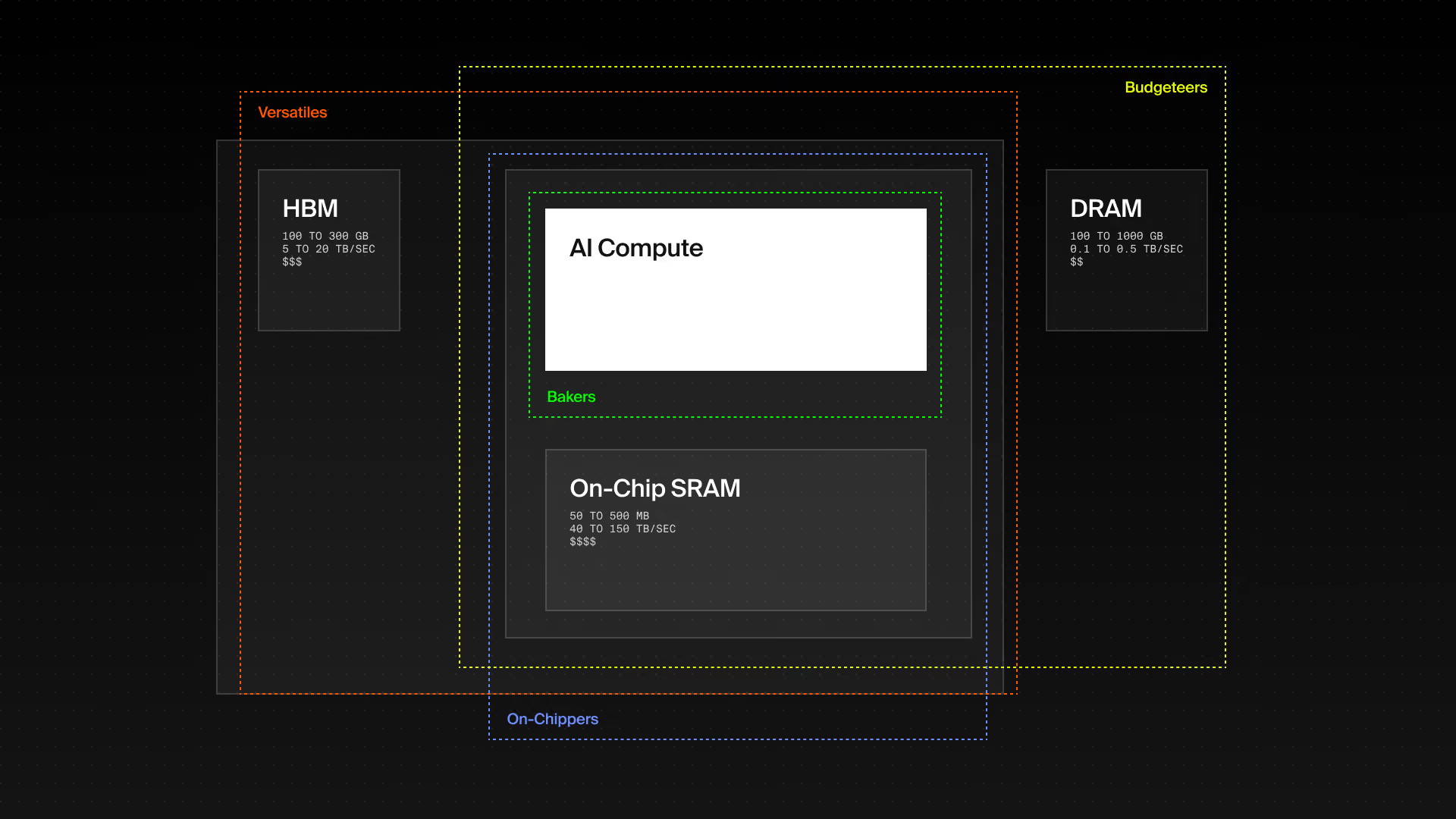
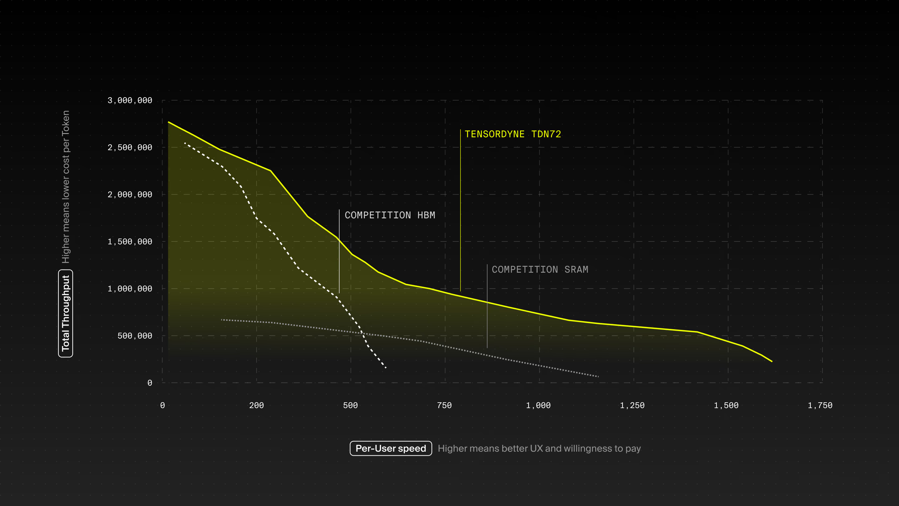
The Bakers
The On-Chippers
The Budgeteers
The Versatiles
The Tokenmaxxers
Depends
Some
Depends
Tensordyne: Napier Deep Dive
Napier was built from the math up. Each design choice gave room to improve the next — from compute, to memory, to interconnect, to the full system. All optimized around what AI models really need.
We have now seen the trade-offs each architecture makes.
Wouldn’t it be great if there was a chip, a technology, a system, a vendor that combined the advantages?
Efficient compute. Fast memory. Large-capacity HBM. Fast, wide, low-latency scale-up. Low power. Low cost.
Logarithmic Math
Shrinks area and power needed for compute.
More SRAM
More SRAM for higher utilization.
Scale-Up Interconnect
Parallelization over 72 chips, no bottlenecking.
Efficient Accelerator
Systolic arrays, Vector Processors and CPU cores.
High-Bandwidth Memory
Large HBM for model size and user context.
That is the Tokenmaxxer bet: Change the math, and you change the trade-offs everywhere above it. Optimize the whole system to get more useful tokens from every watt.
And that is what Tensordyne has spent the last several years building. Napier was designed from the ground up for AI inference, with compounding benefits across all elements of the system:
- Logarithmic math allows Tensordyne to shrink the area and power needed for compute
- The freed-up silicon area and power budget can be used for large amounts of on-chip SRAM, off-chip HBM, and native integration of low latency chip-to-chip interconnect
- Together this enables flexible scaling across all parallelization and disaggregation schemes.
Let’s start with the math.
Math: Replacing expensive multiplication with efficient logarithmic addition
Logarithms are the core idea behind TDN Math. By changing costly multiplications into additions, we achieve a given amount of compute in 3x less chip area and with 5x less power, leading to the world's leading compute per watt and area.
Most if not all AI systems today employ so-called Floating Point number systems to do what AI is all about: Mathematical operations. Whenever you ask Claude a question, or task Nano Banana to generate an image for you - what actually happens is that a giant mathematical formula (called ‘AI model’) gets executed.
AI is essentially all math.
Roughly half of all operations are multiplications (including divisions) and the other half are additions (including subtractions).
Additions are inexpensive. The actual transistor circuit in silicon for adders is small and efficient.
But multipliers are exponentially more expensive (~5x to 30x) than adders (depending on bit-width, architecture, and implementation). Multiplier circuits consume far more chip area (5x to 30x) and chip power (5x to 20x) and have much higher latency (2 to 5x higher) than adders. Hence, they are the culprit.
It is important to emphasize this again:
AI compute is the single largest component of AI datacenter CapEx ($), with GPUs alone accounting for roughly 40% by industry estimates 11 – and around 60% of AI inferencing energy (kWh) 12. Innovation in this space is one of, if not the biggest lever behind making AI more affordable and more energy efficient.
Tensordyne is the first company to have fully productized a Logarithmic Number System (LNS) for AI inference – a way to do math which lets us change multiplications into additions. Log math is both the most accurate (smallest error) and the most efficient, an advantage highlighted by Nvidia’s Bill Dally 13 and others. The idea itself isn’t new. The hard part has always been implementing it in real silicon.
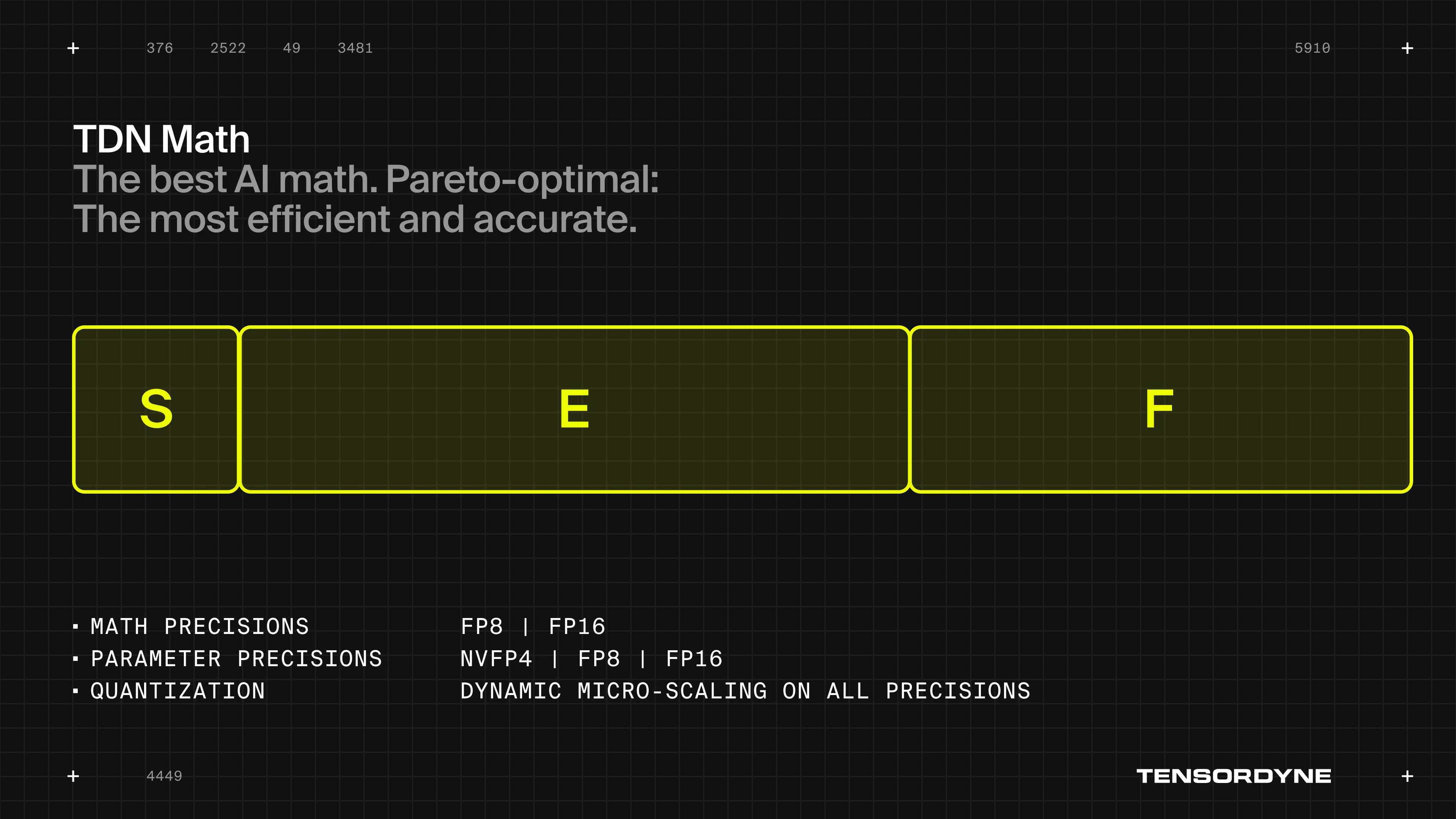
While others reduce resolution for incremental power improvements, Tensordyne’s approach is to maintain accuracy while achieving massive reductions in power consumption. TDN Math allows users to run models in uncompromised 16-bit precision at the power of running it in 4-bit on other systems.
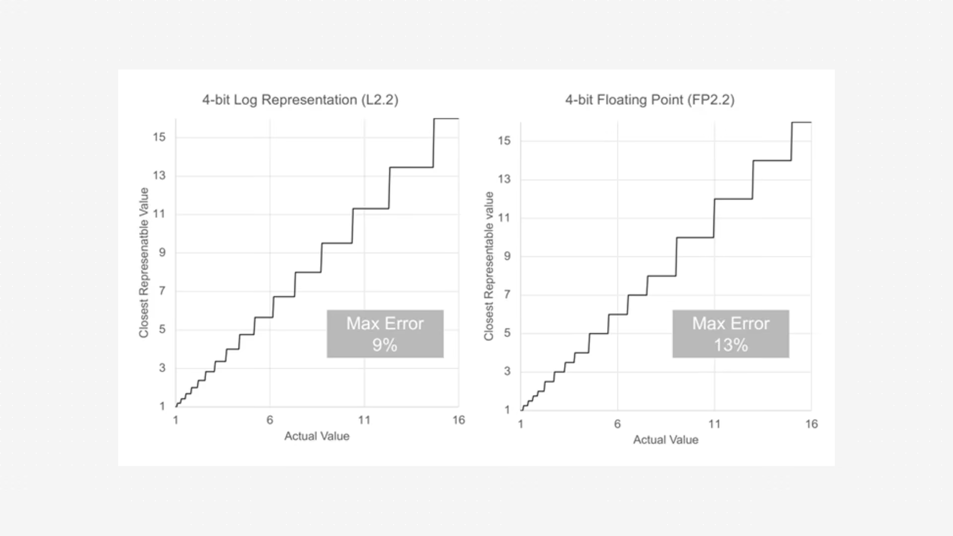
Let’s dive into the nitty-gritty.
TDN Math: How it Works
Intelligence is just Math. We found a better way to do it.
The core idea is simple. Instead of multiplying two “normal” floating point numbers, you are representing all numbers as an exponent of two. So 8 and 16 become 3 and 4 (23 = 8 and 24 = 16) and an expensive multiplication turns into an inexpensive addition:
8 * 16 = 128 turns into 23 * 24 = 23+4 = 27 = 128.
To understand why it matters, let’s start by looking at traditional floating point.
Floating Point Math: The Traditional Approach
Floating Point is a number system that represents numbers in the form of -1S * 2E * (1+F). It is the favored format used in AI XPUs for training and inference. Here E is the ‘exponent’ and F is the ‘fractional’ part (i.e. a number smaller than 1 often referred to as the ‘mantissa’), and S is the ‘sign’ (1-bit plus or minus). For an 8-bit number using 4-bits for the exponent and 3-bits for the fractional part we get the IEEE Standard 8-bit Floating Point notation: S1E4F3.
Now when two Floating Point numbers are multiplied (dropping the sign for simplicity) the formula reads as:
From a silicon point of view, the right-hand side of the above equation requires the following:
Adding E1 and E2. Multiplying F1 * F2 and adding the result to 1 and F1 and F2. Finally, shifting the right-hand formula’s result by E1+E2 (an integer number by definition) to the left.
So in total we’re looking at 4 additions and 1 multiplication. And then another barrel shifter (okayish-ly expensive circuit in silicon) for the final bit-shift.
As one can see, the number of bits spent on the fractional part (F) of the number defines the cost of the multiplicative portion and increases quadratically with the number of bits ‘n’ (O(n2)). Therefore, the lion’s share of the overall cost is multiplication for 8-bit Floating Point (FP8) numbers.
BF16 is another common Floating Point format supported by modern AI chips, such as GPUs. BF16 has the notation S1E8F7, making multiplications even more expensive than FP8 while still being less accurate than IEEE standard FP16 (S1E5F10) - or in other words a compromise out of necessity.
TDN Math: Changing multiplications to additions
Numbers in TDN Math are represented in simple LNS (logarithmic number system) format: -1S * 2E.F.
A multiplication becomes simple (again dropping the sign):
A single addition. That’s it. Eliminating multiplier circuits from silicon. A straight-forward idea.
Then why isn’t everybody doing it? Because the ‘problem’ now shifts since there are additions that follow nearly every multiplication in AI models that would need to be done in LNS representation. And it turns out that is pretty complicated.
Then how do we solve this?
If we can make linear-to-log and log-to-linear transformations inexpensive and fast in silicon and accurate, then we can do the multiplications in log space (as additions) and the additions in linear space.
Until now the issue is that one would need very expensive operations to implement Logarithmic Math in this straightforward way: first a 2(..) and then a log2(..) operator. Whether through Look-Up-Tables (LUTs) or through Taylor Series implementations, it would be so expensive to implement that, bottom line, nothing would have been gained.
And this is exactly the main reason why some bigger companies gave up on it at some point: Whatever was saved during multiplication, was over-spent in conversion.
Tensordyne solves this by employing an evolved version of the Mitchell Approximation (famously used by John Carmack in Quake3 to solve the inverse square root problem), which in its original form reads as:
log2(1.X) = 0.X
or
2(0.X) = 1.X
In silicon this means “when you have a number that comes in the shape of 1.X, you can just throw away the leading bit (‘1’) and you have successfully turned that number into its logarithmic state.” In other words:
Practically zero cost.
Did you catch it? It’s easier to see by comparing LNS and FP formats side-by-side (again dropping the sign bit):
LNS: 2E.F = 2E * 20.F
FP: 2E * (1+F)
Note: In order to arrive at a number in the shape of 1.X even if the number is higher or lower than 1.X, one simply has to factor out an exponent of 2, which can be easily done on the chip by identifying the MSB and then shifting accordingly.
Does it really work?
Tensordyne’s first TSMC 7nm prototype chip implemented LNS in its original version and was able to prove it was the most energy efficient AI chip on the planet, beating competition like Nvidia and Qualcomm by 7x to 30x in 3rd party case studies 14.
The issue with the entire ‘vanilla’ implementation normally would be the error it introduces (Figure 18: the difference between the white ‘belly’ (solid line) and yellow (dotted) line in the left graph below). It’s the Mitchell Approximation after all.
For our first chip running smaller models, error could be compensated for through QAT (quantization aware training), however, this isn’t economically feasible for today’s massive models.
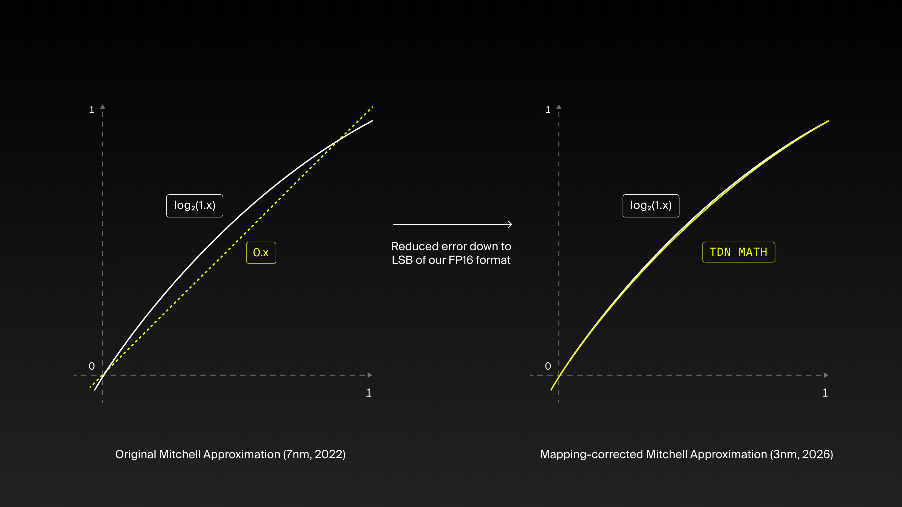
So now, TDN Math is taking it to the next level.
By massively improving the Mitchell Approximation through low-level mathematical error adjustments (Figure 18: essentially bringing the white ‘belly’ (solid line) and the yellow (dotted) line much, much closer together in the right graph), we have successfully reduced the error down to the precision level of FP16 (< 0.08% error).
These error adjustments are extremely fast and inexpensive in silicon for both linear-to-log and log-to-linear transformations, enabling TDN Math to eliminate the accuracy penalty of logarithmic math without giving back its efficiency advantage — an approach innovative enough to earn Tensordyne a US patent.
And it happens automatically under-the-hood – you don’t need to do anything. Complexity is completely hidden from the user. Manual fine-tuning is possible through software - but is entirely optional. TDN Math is a purely PTQ (post-training quantization) approach and provides a calibration-free / retraining-free experience.
And most importantly we’ve proven down-stream task accuracy through years of R&D and extensive verification with real workloads. We’ve performed countless bit-accurate emulations covering all modalities (dense LLMs, MoEs, and image, audio, and video generation), model sizes (Llama 8B to DeepSeek V4 Pro and KimiK3) and context lengths (1K to 1M). So you can be 100% confident in TDN Math.
TDN Math: Architectural Advantage
What does TDN Math get us? Everything. Area, power, speed, cost per token. Everything inherits the benefit, because the saving happens at the level everything is built on top of.
On a silicon-level, TDN Math achieves an industry-leading compute density of up to 20 TFLOPS/mm2 for dense FP8 math - with other XPUs consistently well below 10 TFLOPS/mm2 - and a power reduction of 5 to 20x.
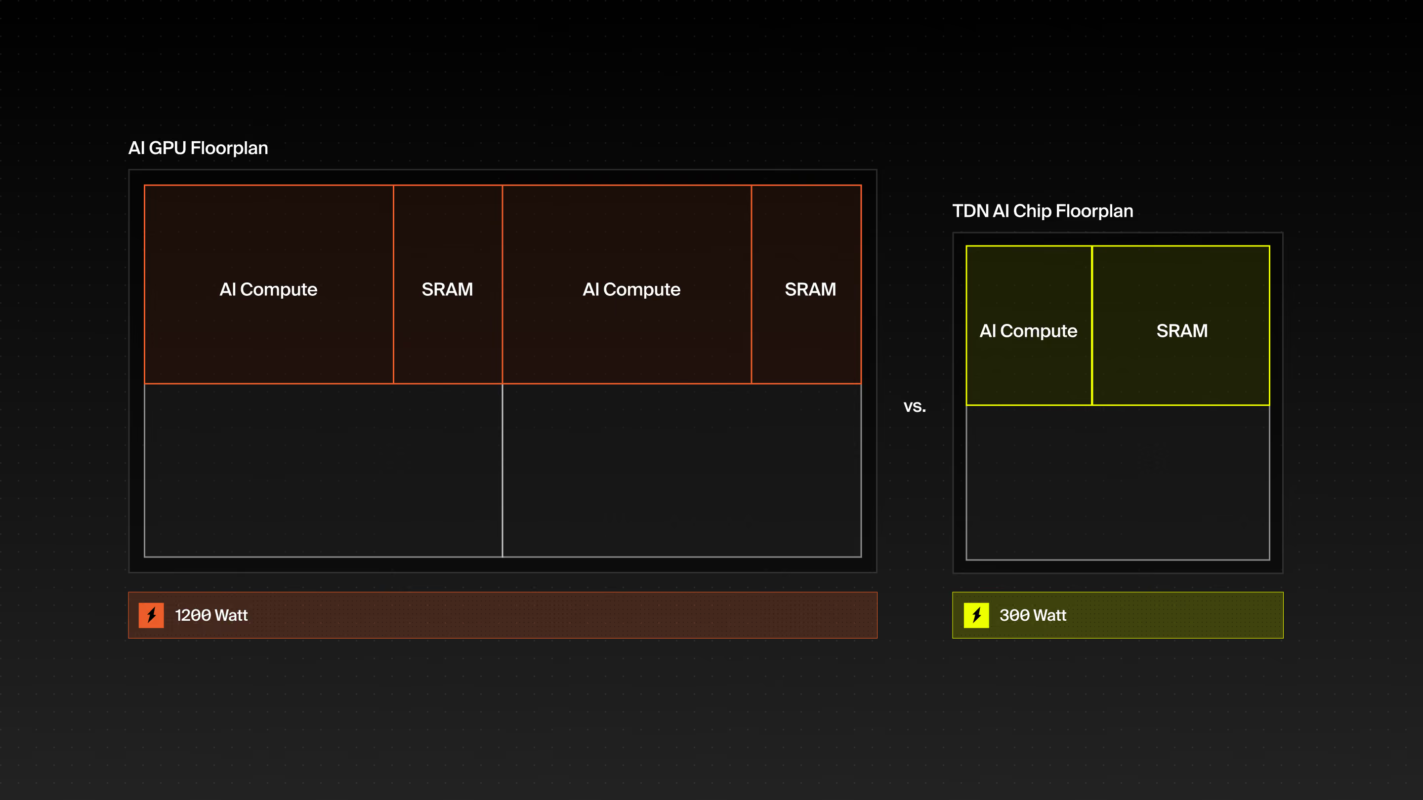
This massive reduction in compute area and power compared to Floating Point (see figure above) has much broader implications, enabling us to create a much more balanced design by increasing the amount of on-chip memory, including more general-purpose CPU cores, widening data-paths to eliminate any bottlenecks and integrating the fastest chip-to-chip interconnect the world of AI compute has seen. More on these topics later. But first, let’s go beyond the math and look at some other compute optimizations.
Compute: Right-sized for inference, not inherited from training
One chip for both prefill and decode. Compute designed together with memory and interconnect. Compute only matters if you keep it busy.
Our compute innovations don’t end with log math.
Our AIP (Artificial Intelligence Processor) has a novel vector processor unit (VPU) that works completely in parallel with our MatMul systolic array to optimize AI inference. The VPU takes care of all non-MatMul operations and includes highly optimized execution of complex functions like Softmax, etc. Both are compiler-scheduled and highly deterministic to eliminate wait states and work together for maximum utilization.
Tensordyne supports all of the dominant number formats used today including BF16/FP16, FP8 and NVFP4/MXFP4. We have automated on-the-fly quantization (microscaling) which dynamically derives heuristics of a group of numbers and then scales that group’s number range appropriately. This ensures high numbers are representable while smaller numbers get all the precision they need. The experience deploying models has been prioritized.
In every design phase we find opportunities for improvements, whether custom accumulator designs to deliver higher accuracy at lower cost or multi-instruction queues and optimized layouts to reduce energy costs of data movement.
We could have easily put more compute on the chip than we did. But our focus is to keep compute fed and increase utilization to maximize the effective performance for inference rather than the specifications. What good is it to have more compute that is sitting there idle because other parts of the system are bottlenecked?
Memory: Large HBM and unusually large SRAM on the same chip
Memory capacity and bandwidth have to be considered together. And on-chip SRAM has an outsized impact on utilization and programmability.
Compute implemented as Floating Point takes up so much space on silicon, that it has been very hard or even impossible to build XPUs that offer both HBM and also a large on-chip SRAM.
TDN Math isn't just an algorithm. It's a land grab. It shrank the area for compute so we can give you the most optimized SRAM-to-HBM ratio in history.
A single AIP comes with 256 MB of SRAM at 40 TB/s and 144 GB of HBM at 4.7 TB/s turning it into the most versatile compute node: Able to work as a workhorse for lowest cost and highest amount of parallel users while also offering the benefits of high-bandwidth SRAM for the compiler to work with, store intermediate results without going off to HBM, etc.
With globally rising memory prices, a balanced memory architecture in combination with efficient math has never been more important or a bigger lever than ever before.
Interconnect: Low latency, high bandwidth, and predictable behavior
TDN Link is our scale-up fabric that provides any-to-any connections for up to 72 chips and is Tensordyne’s proprietary answer to NVLink. It tackles one of the hardest challenges of serving large AI models at fast speeds.
Tensordyne AIPs (Artificial Intelligence Processors) connect to each other through TDN Link, our patented cell-based any-to-any scale-up fabric, which is integrated directly into each AIP.
Each AIP has 1 TB/sec of bi-directional bandwidth and a hyper-low single-hop latency of less than 1.5 microseconds. Workloads scale nearly linearly across 72 nodes using all forms of parallelism 3.
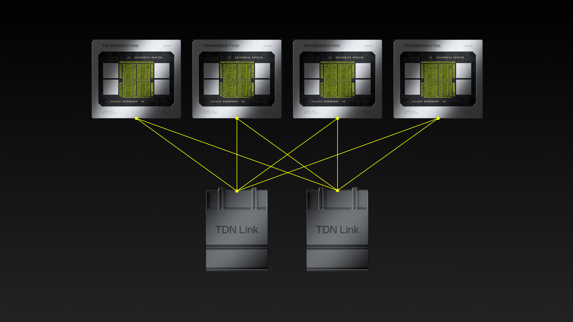
Raw bandwidth and nominal latency are important metrics for scale-up fabrics. But for intense AI workloads, real-world performance is heavily driven by congestion and tail latency.
Scale-up fabrics execute lots of synchronous collective operations (e.g., All-Reduce or All-to-All). In those cases the whole cluster can end up waiting for the slowest transfer to finish. So average latency only tells part of the story. What really starts to matter is the worst-case tail latency – especially as you move from 8 to 16 to 32 or 72+ nodes.
Traditional interconnect architectures, including packet-based implementations of NVLink and Ethernet, use variable-length packets. This can lead to Head-of-Line (HoL) blocking, where large transfers can get in the way of smaller, time-sensitive ones – effectively blocking communication until the entire "packet train" clears.
TDN Link takes a different approach. It is cell-based and uses a divide-and-conquer approach that slices data into small, uniform "cells" that are routed and interleaved automatically. This allows the fabric to handle congestion dynamically and predictably, keeping tail latencies much closer to nominal. This delivers near-linear scaling even under bursty, random traffic patterns like those found in large-scale Mixture of Experts (MoE) workloads.
We also take software out of the critical communication path. While conventional XPUs typically rely on runtime abstraction layers such as NCCL to coordinate collective communication, TDN Link operates without CPU involvement. Communication primitives are handled natively in hardware through dedicated microcode engines.
Less overhead. Less jitter. More predictable. Clock-cycle-accurate fabric behavior with bare-metal efficiency.
And the entire electrical, mechanical, and overall technological concept behind TDN Link is highly reliable with a proven uptime of 99.999%.
No cables. No optics. Just PCBs and connectors.
TDN Link is fault tolerant so the TDN72 can keep working with reduced bandwidth in the case of a switch failure. Getting the system back to full speed is just a matter of hot-swapping cards resulting in minimal downtime.
Chip Architecture and Control Flow: Making it all work together
Before diving into our TDN system performance, let’s review the silicon-level design choices we made and how they make it possible to scale inference across 100+ chips without creating new bottlenecks.
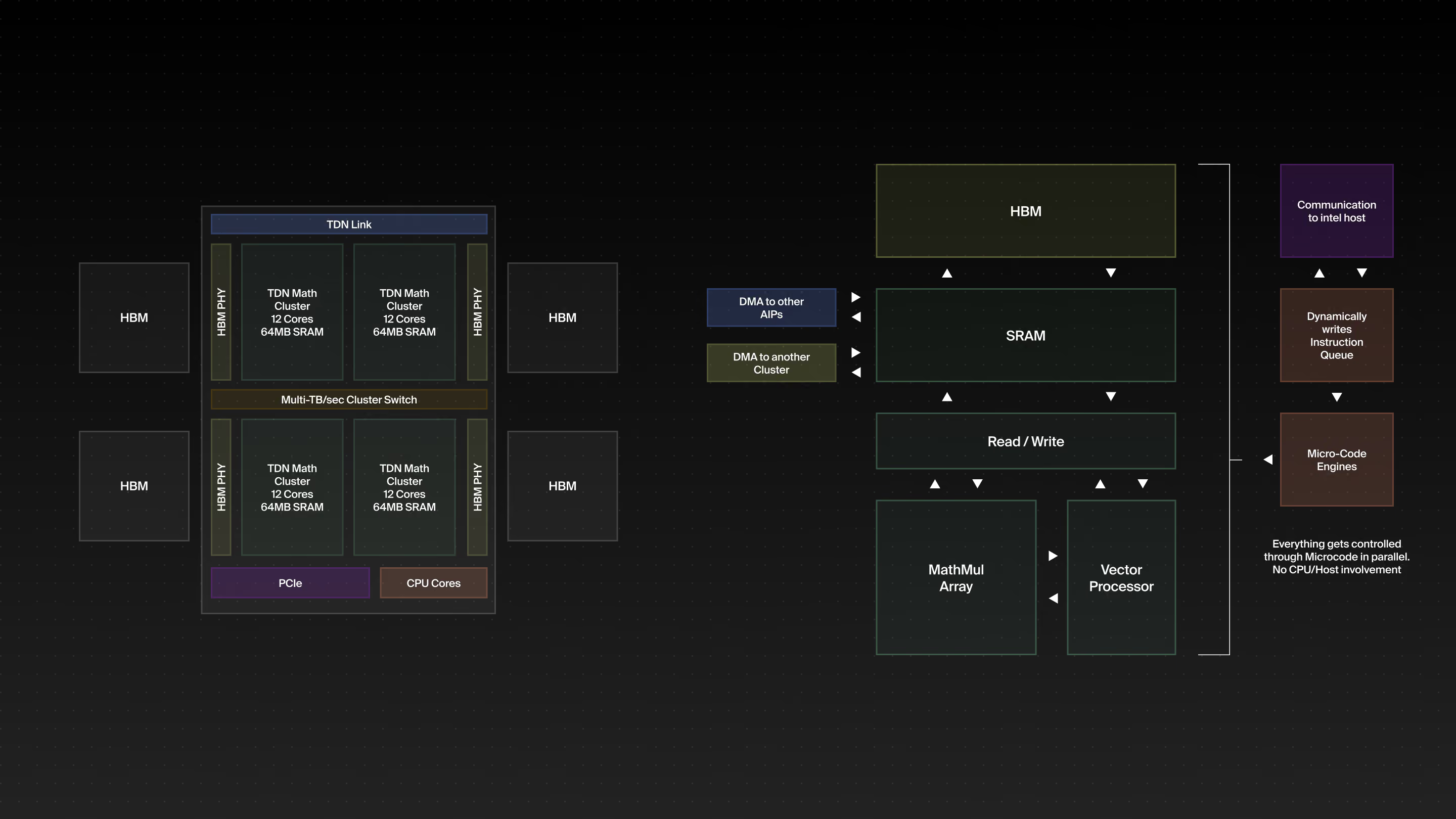
The advantages of our approach can be summarized as follows:
- Our TDN Math compute clusters can always keep up with the data they receive from (or writes into) their adjacent HBM memory module (~1.2 TB/s)
- The four compute clusters talk to each other at a speed that surpasses HBM bandwidth - such that in extreme (rare) cases cluster A could work on data from cluster B’s HBM - without hitting a bottleneck
- CPU cores are out of the mix. They dynamically patch instructions into the queue (e.g. MoE routing, batching, ISL/OSL changes, precision-selection changes etc.) but execution speed is never gated by CPU speed - everything is controlled by microcode engines.
- Talking to other clusters or to another AIP works in the same way - both are DMA-based. Data flow to another AIP through the scale-up fabric is handled without software/ host involvement.
We tried to simplify things as much as possible, without sacrificing performance or programmability for it. The result is that this design is fundamentally more streamlined and easier to program than any other design we have seen.
Software: Making a new architecture practical to deploy
Software has to be easy. Customers don’t want a separate stack for every new AI inference system. Napier supports the frameworks and tools they already use.

Deploy a model from our model hub, hosted on Hugging Face. Our SDK seamlessly enables fine-tuned models as well.


Compile a model that is defined in a mix of PyTorch and Triton.
Implement a model directly in our Python eDSL (tensordyne.nn).
We’ve heard from customers ranging from small Neoclouds to large Hyperscalers that integrating new AI inference vendors has to be easy to implement and manage through a single software stack - not a separate stack for each vendor.
You’ll get exactly what you want from Tensordyne:
- Hugging Face hub - for those who want to directly deploy pre-optimized open-source models or as a starting point for your own special fine-tuning
- PyTorch, Triton - for those who want to quickly turn around custom models already defined for Nvidia and AMD systems
- Tensordyne.nn – our own eDSL that lets developers define deterministic kernels on the lower levels of silicon and system control - mostly targeted at frontier labs that demand highly optimized control
Inference Server-wise we expose clearly separated Runtime and Telemetry APIs. vLLM and other inference servers can connect directly. So TDN easily fits into your K8s-managed multi-vendor datacenter.
Agentic Kernel Optimization
Another important topic from 2026: We are recognizing huge potential from using AI agents to make software support for new models faster. Give an agent the right documentation, examples, compiler feedback, and access to real hardware and let it iterate to close the gap between generic open-source frameworks such as PyTorch, kernel languages such as Triton, and custom ASICs with their own eDSL/IR/ISA like our TDN AIP.
The basic idea: An AI coding tool might not get translation of a new DeepSeek or Kimi – or any other model that was just released – right or sufficiently performant on the first try. But an agent can:
- verify numerically through test vectors if it’s doing the right thing
- profile compiler-generated executables against speed requirements
- measure actual performance on real hardware
- iterate until performance meets end-user targets
Tensordyne will include multiple AI-based capabilities like these in our release SDK to make life easier for end users.
Tensordyne: Napier Performance and Economics
Fast is good. Fast and cheap is what matters. Power limits them both.
The fight of the bottlenecks is real. When running models on modern AI systems, the system will usually run into at least one of the five bottlenecks:
- Compute-bound
- Memory-bandwidth-bound
- Memory-capacity-bound
- Fabric-bandwidth-bound
- Fabric-latency-bound
Any of these five bottlenecks can cause a system to not scale beyond a certain speed or cost effectiveness or capability and push vendors to develop multi-vendor disaggregated systems to attempt to address shortcomings.
Tensordyne’s TDN72 – with 72 TDN AIPs incorporating TDN Math and TDN Link as core technologies – is able to operate in ways in which all five bandwidths/traits are most equally leveraged.
Let’s look at how Tensordyne Napier compares for two model examples, starting with a look at key rack-level performance characteristics. 3
Rack-Level Comparison
More tokens. Faster tokens. Less power. Success depends on all specs, not just one.
On a per-rack basis a Tensordyne Napier system with 4x TDN72 pods delivers strong specs across the board compared to Nvidia, while keeping the overall system right-sized for inference.
Rack Specification
Tensordyne TDN72 x4
Nvidia Blackwell NVL72
Nvidia Rubin NVL72
Nvidia Groq 3 LPX
Fabric Bandwidth
275 TB/sec
130 TB/sec
260 TB/sec
640 TB/sec
Fabric Latency (hop)
<1.5 µs
~10 µs
~10 µs
~10 µs
SRAM Capacity
72 GB
<10 GB
<10 GB
128 GB
SRAM Bandwidth
11.5 PB/sec
<2 PB/sec
<2 PB/sec
38.4 PB/sec
HBM Capacity
41.5 TB
20.7 TB
20.7 TB
NA
HBM Bandwidth
1.35 PB/sec
0.58 PB/sec
1.58 PB/sec
NA
Compute (FP8 dense)
608 PFLOPS
360 PFLOPS
1260 PFLOPS
315 PFLOPS
Power (max)
120 kW
150 kW
240 kW
154 kW (est)
Racks Needed:
2T model, FP4 weights
1
1
1
8
Tensordyne combines traits of On-Chipper and Versatile systems into one technology, one chip, and one rack - essentially introducing a new class of AI inference systems: The Tokenmaxxers.
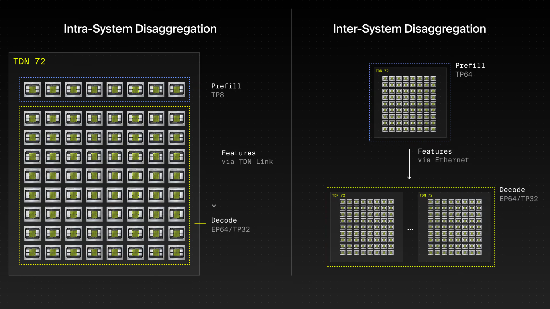
When we look closely though, the advantage becomes more pronounced for multi-vendor disaggregated systems which require multiple On-Chipper racks to achieve higher per-user performance for large models, while a Tensordyne TDN72 can support both intra- and inter-system disaggregation with a single homogeneous architecture. In fact, Tensordyne is the only vendor at this point that supports all forms of disaggregation.
Rack Specification
Tensordyne TDN72 x4
Nvidia Rubin NVL72 + Groq 3 LPX
AMD Helios + Cerebras CS-3
Racks Needed:
2T model, FP4 weights
1
1 + 8
1 + 12
DeepSeek-R1 and Future 2T Parameter MoE
Active weights per node and fabric latency can dominate high-speed decode.
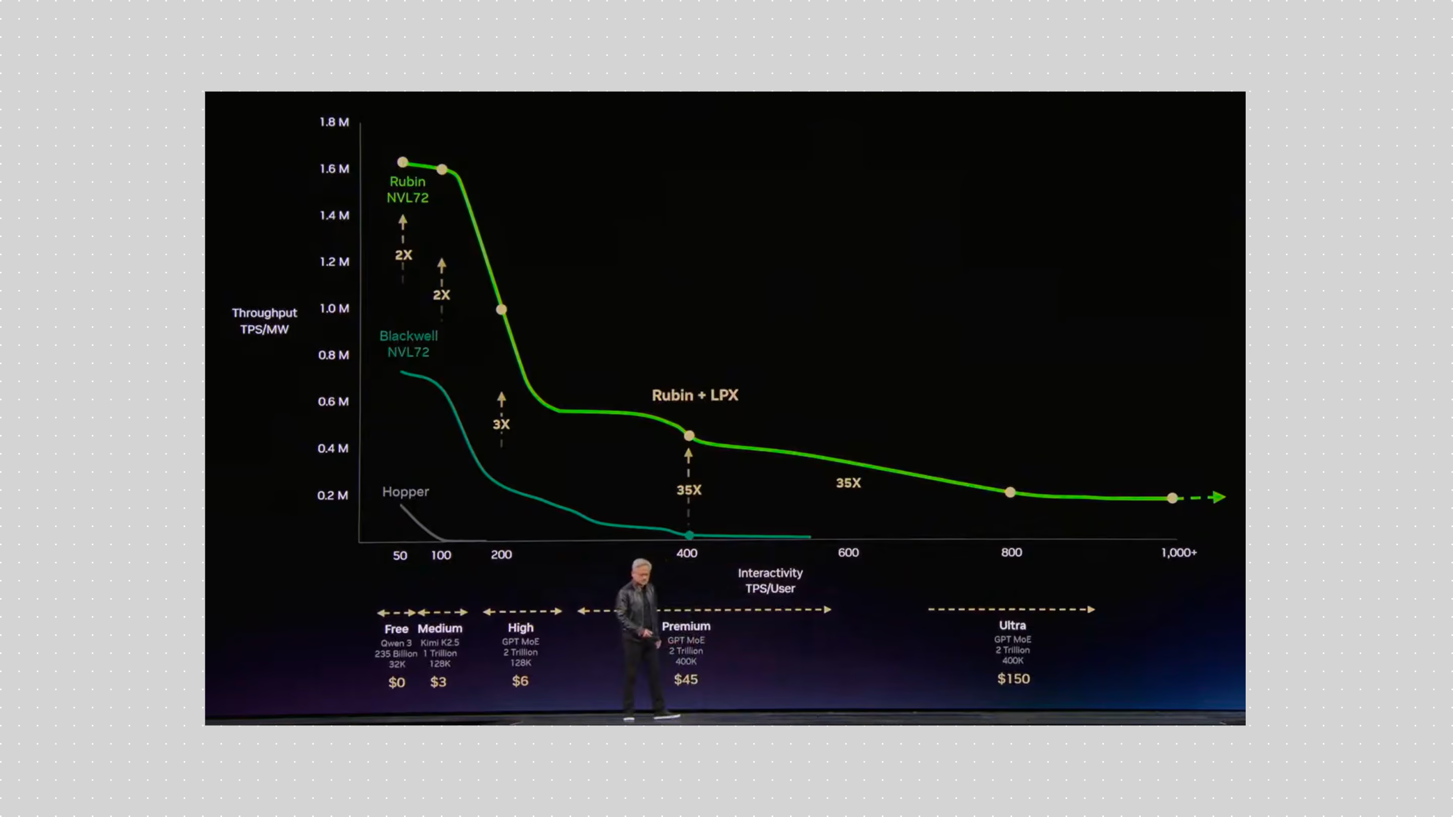
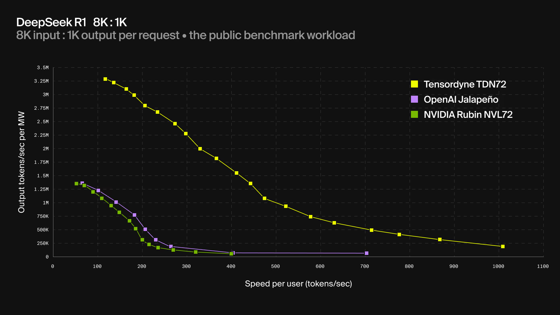
The above graph from the GTC 2026 Keynote shows Nvidia projections for the Vera Rubin + Groq LPX system performance (throughput per MW vs. user tokens per second or interactivity). It also provides potential pricing for different model sizes, suggesting that increasing model size combined with demand for higher per-user speeds will result in massively increased price points for the multi-trillion-parameter models. While it is clear that model sizes will continue to increase, $150 USD per 1M tokens is not a viable price point.
In order to derive model performance for today’s leading models, we have to focus on Decode: the part that drives cost and must be optimized to deliver high per-user speeds.
Model Architecture
Mixture of Experts (MoE) models have become the dominant architecture due to their computational efficiency, scalability, and task specialization enabling them to deliver better results. MoEs pick the best-suited subset of “experts” for a specific request, instead of having to load every model weight. But this also results in significant implementation challenges when trying to achieve highest user speeds in decode. Together this makes MoEs ideal for comparison.
So let’s look at two MoE model architectures:
- DeepSeek-R1 – the 671B parameter open-weight reasoning model which shook the AI industry by showing that open-weight models could deliver performance rivalling proprietary models but at much lower cost
- 2T GPT-like MoE – our attempt to define a challenging model architecture to compare with the “GPT MoE 2 Trillion parameter” for which Nvidia’s Jensen Huang shared projected performance of the Nvidia Vera Rubin + Groq LPX system at GTC 2026.
Model Architecture Spec
DeepSeek R1
2T GPT-like MoE
Total Parameters
671 Billion
2000 Billion
Layers
58
100
XPU to XPU communications per Decode Token
232
400
Parameter Precision
FP4
FP4
Activation Precision
FP8
FP8
Routed Experts
256
512
Shared Experts
1
1
Active Experts
8
16
Expert Parallelism Degree
64
64
Tensor Parallelism Degree
32
32
Parameters to load per node at BS=1
0.32 GB
0.95 GB
Parameters to load per node as BS=2
0.48 GB
1.43 GB
Parameters to load per node as BS=8
1.45 GB
4.32 GB
Parameters to load per node as BS=64
5.32 GB
15.86 GB
What’s important to note is how the amount of parameters to load from memory increases steeply with a growing atomic batch size, since there is a higher statistical likelihood for more experts to be activated as the number of parallel users increases.
In other words: at e.g. a batch size of 64, it is almost 0% likely that all 64 users are using the exact same experts.
Hence by processing only a few users in parallel – e.g. BS=2 for the 2T model – one can get away with “just” HBM bandwidth to load weights fast enough and still maintain a 1000+ OTPS (output tokens per second) per user — as long as the fabric latency can keep up.
At high degrees of EP and TP, in combination with a low batch size, the fabric latency is by far more important for system performance than fabric bandwidth since the packages exchanged between XPUs are extremely small, yet frequent.
To take an example, at a batch size of 2, the total of 2.39 Gigabytes of parameters can be loaded within 0.51 milliseconds through our HBM3E interface - putting the theoretical OTPS ceiling at 1/0.51ms = 1960 Tokens/sec.
In this scenario, even though we are in a traditionally bandwidth-bound phase of execution (Decode), the time it would take to compute all the necessary math teraFLOPS for this XPU node would be slightly higher at ~0.6ms (depending on context) - essentially overshadowing the weight loading time. At a batch size of 3 this would already flip into an actually bandwidth-bound situation.
Note how the above rationale is exactly the same as Groq’s concept - but without the need of extra hardware:
Let’s speed up parameter loading so much that Decode becomes a compute-bound problem again.
Why ultra-low fabric latency matters
At low batch size, messages can be small enough that transfer time is secondary. The fixed latency paid hundreds of times per token can become the governing limit.
However - the 232 fabric communications that need to take place for every Decode token define another ceiling:
If we want to keep the system still memory-bandwidth-bound at ~2000 tokens/sec (=0.5ms), then single-hop latency cannot take on average longer than 0.5ms / 232 = 2.2 microseconds.
Note: the bandwidth is almost irrelevant here, because at high per-user speed batch sizes are fairly low. As long as batch sizes are below ~16-32, the time it takes to exchange the necessary feature vectors is so small compared to the latency cost of every hop that it remains an entirely latency-bound system.
Our system is the only one in the industry with a single-hop latency lower than 1.5 microseconds. Not just in the best cases. But on average! Thanks to our patented cell-based fabric approach we are massively beating NVLink latencies which typically all-in reach up to 10 to 13 microseconds.
Note how NVLink is thereby a bottleneck in wide expert and tensor parallelism deployments, which is exactly the reason why Rubin relies on Groq racks to reach higher user tokens per second.
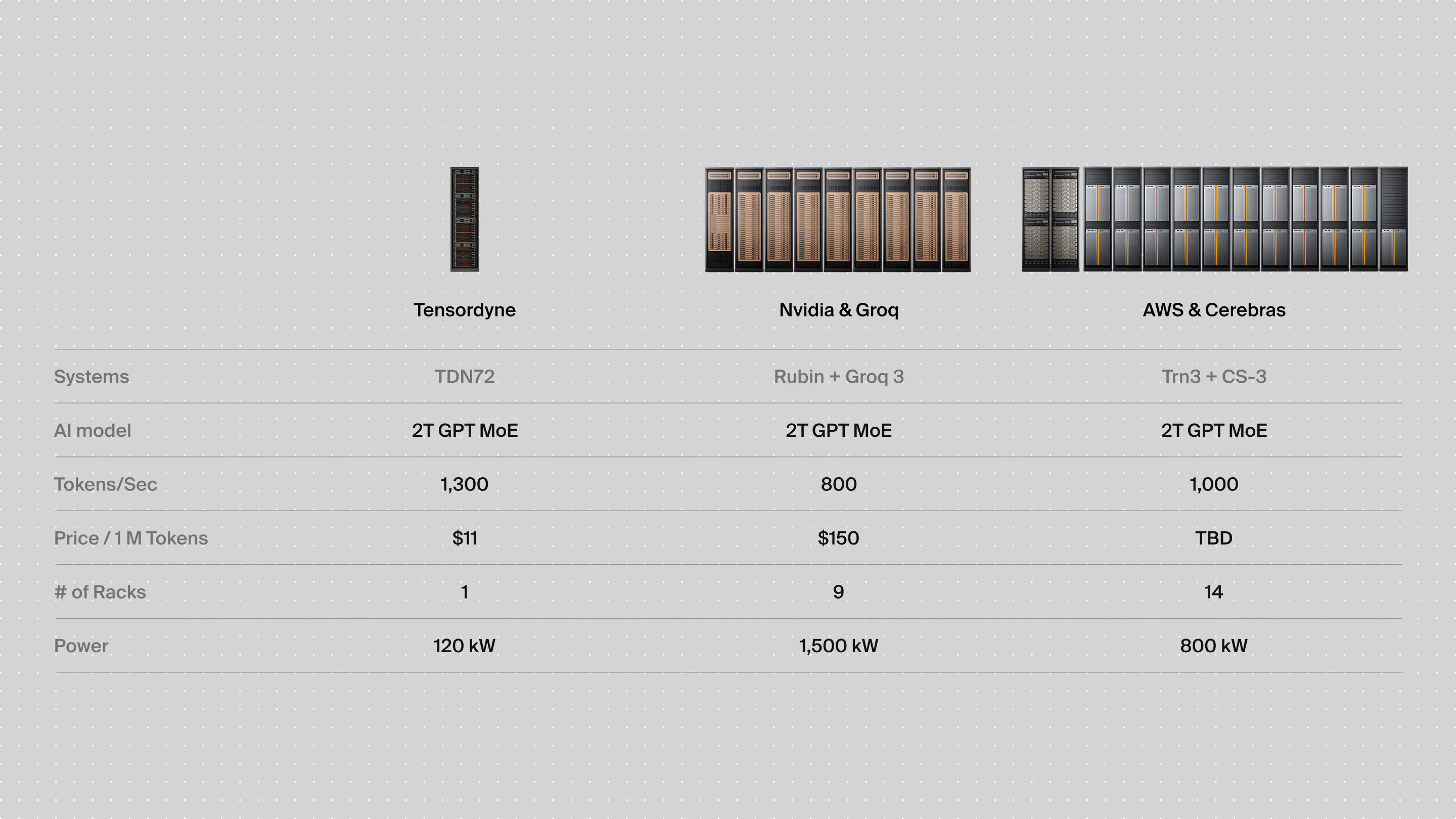
The result is an entirely different footprint in the datacenter, as shown above: Nine racks of Nvidia+Groq or 14 racks of AWS+Cerebras compared to a single Tensordyne Rack with 4x TDN72 pods.
Performance and Economics
Running those large MoE models on Tensordyne Napier vs Nvidia’s platform results in the following Per-User Speed and Cost roofline KPIs.
DeepSeek R1
2T GPT-like MoE
Tensordyne TDN72
Nvidia Blackwell
Tensordyne TDN72
Nvidia Rubin + Groq
Low Cost Mode
Tokens/Sec p. User
800
30
296
200
TCO in $ / 1MT
$0.70
$1.00
$1.50
$6.00
Batch Size (users)
64
1024
64
N/A
High Speed Mode
Tokens/Sec p. User
1200
285
1300
800
TCO in $ / 1MT
$1.50
$4.00
$11.00
$150.00
Batch Size (users)
16
N/A
2
N/A
What is striking about the above comparison is that a single system and chip architecture (Tensordyne TDN72) – which would usually imply that a set of compromises had to be made – could actually significantly outperform a system assembled from two specialized sets of hardware (Rubin+Groq).
That is the Tokenmaxxer approach: get the whole system right, and you don’t need to bolt together two different ones.
Tensordyne: Ready for Today, Future Proof for Tomorrow
Napier scales from a single AIP to a 72-chip system, and from there to multi-pod deployments built for even larger models and world sizes far into the future.
Agentic AI: From Chat to Real Work
Large MoEs are one proof point. But Tensordyne Napier also aligns perfectly with agentic workflows.
At the onset of the age of agentic AI, AI model execution has become messier, longer, more random, unpredictable and sparser than ever. As a result, AI compute utilization is at an all-time low. Globally GPU utilization 24/7/365 is hovering well below 10% - maybe as low as 1% if you actually counted idle cycles on the most atomic level. You simply never know when that prompt, that request, that agentic task is going to happen - but you always want an XPU on stand-by, ready to compute when you need it. Maintaining clean, secure multi-tenant serving at high average compute utilization is a real struggle for many TaaS (Tokens-as-a-Service) API providers.
The best way to improve agentic performance is:
- Run AI in maximum precision: Spend 16-bit where it makes sense, to reduce the statistical likelihood of hallucinations/low-quality answers and generally to eradicate compromises on multi-modal reasoning.
- We do realize that FP8 and FP4 are on the rise. But for us doing 16-bit decode comes at practically zero cost - and we do see that outlier performance benefits from this quite a bit.
- Even the newest releases like Kimi-K3 actually still use 16-bit in many places throughout the model like context and normalization
- Run the biggest (and thereby best) models available. A 10T parameter model will beat a 100B parameter model in the long-run. But it needs to be both fast and affordable.
- Keep all models of a stack close. Having multiple models of an agentic stack communicate through TDN Link within a single system, instead of spreading it over multiple CSPs and geographies has a huge impact on tail-latency.
- And most importantly: Optimize AI inference compute for agentic tasks. Most agents have a huge input-to-output-ratios of more than 100:1, and large parts (north of 90 to 95%) of the input context are KV cache hits (meaning: loading pre-computed KV caches that are often used and hence stored for reuse). The key to that is:
- Large and(!) fast memory pools that allow the co-existence of hundreds if not thousands of long contexts - all concurrently living in the same giant memory pool (e.g. 100-1000 XPUs with HBM) - ready to be accessed at less than 100ms of transfer time
- Rethinking parallelization and cache sharding schemes to maintain high Decode output token speeds when large KV caches have to be reloaded for every Decode token
- Make sure your entire silicon-to-inference-server stack can handle batch sizes of at least 8 to 32 effectively on an atomic level
Tensordyne offers all three in a single system. Ready for the wave of agentic AI adoption that is about to disrupt most if not all business models as we know them today.
Real-Time Video Generation: The Next Big Thing
Agentic AI is huge. Real-time video could be even bigger.
Text-to-text LLMs still represent the core and heart of most AI stacks, but other content generation modalities including image, audio, and video are gaining traction and will likely surpass Agentic AI as the fastest-growing segment in the next few years.
Real-time / Conversational AI Video
- Digital AI Twins
- Education / Teachers
- Consulting
- Therapy / Coaching
- Digital Friendship / Romance
- Corporate Training
AI Content Creation
- TV / Streaming Services
- Social Media
- Advertisement / Marketing
- Product Visualizations
Physical AI Video
- World Models
- Robotics Training Data
- Synthetic Video Training Data
Video is the most interesting, as it is by far the most computationally demanding as well as the most promising for lifting AI capability to the next level.
The world is full of video data that AI has barely started to use – for learning, as input, or as something to generate. And generating video is totally different from generating text. Every frame requires tons of math spread across many XPUs. That makes it super important to scale that compute efficiently.
State-of-the-art models such as Wan2.2, a non-autoregressive DiT (Diffusion Transformer), are mostly compute-bound - as long as spreading them over e.g. 64 chips does not result in a communication bottleneck.
Hence Tensordyne TDN72 systems can accelerate video models at high frame rates and affordable price points – not just large LLMs.
TDN72 will accelerate Wan2.2 at 4K at 30 FPS, at < $100 per hour of generated video material 3.
Real-time video.
Today’s models are not there yet. But once quasi-infinite attention, auto-regressive frame-to-frame generation and an overall consistent cinematic quality have been figured out (we are projecting this to happen within the next 18 months), Netflix, Instagram, YouTube, Prime Video and co will enter the age of ad-hoc, real-time generated state-of-the-art video generation.
And video generation will continue to progress toward world models: AI models that don’t just generate clips but continuously build and update interactive representations of the world. Media generation and simulation start to converge into persistent, real-time environments that users and agents can explore and interact with.
And that takes a huge amount of compute. Bigger models, longer context, persistent state, and continuous generation all push beyond the limits of a single system – requiring much larger world sizes for AI inference.
World-Size 1000 and Beyond: The Future of Scale-Up
Bigger models. Longer contexts. Agentic AI. Real-time video. Inference is outgrowing a single system.
Large-scale clusters have been common in AI training for years. Inference is now heading in the same direction. Large MoEs, agentic AI, real-time video, and world models will increasingly benefit from world sizes beyond one 72-device domain.
Scaling is easy. Fast scaling is hard.
The trick is to keep the most latency-sensitive work inside the pod, while using fast external switches to connect multiple pods together. Intra-pod and inter-pod communication are different problems — and have to be treated that way.
Larger MoEs lend themselves extremely well to large world sizes. Think: a 5T parameter MoE with 1024 experts, one expert per node for fastest-per-user speed. That creates the next-stage scale-up challenge:
Connecting many pods together while still maintaining any-to-any connectivity and keeping latency and bandwidth – latency being more important – at satisfying levels.
This requirement is the backbone of the continued evolution of the world’s best frontier labs. It’s the only way they can keep making their models better – and thereby larger – while maintaining blazingly fast per-user speeds. Higher speeds help support >>$10/1MT premium pricing, which helps fuel the next generation of models. It’s a delicate loop of evolution. And hardware is at the base of enabling it.
That is where Napier’s multi-pod architecture comes in. Napier extends the architecture by replacing selected ACT compute trays with scale-up trays that provide pod-to-pod connectivity.
Tensordyne offers a seamless, quasi-infinitely scalable solution to this.
Tensordyne Napier Ultra — Scale-Up Beyond a Single Pod
Napier Ultra extends Tensordyne scale-up from a single TDN72 pod to 16 pods or more — creating one AI inference system with a world size of 1,000+ chips.
By replacing ACTs with our SUTs (Scale Up Trays), Napier Ultra extends TDN Link connectivity beyond the pod with 6.4 Tbps of inter-pod bandwidth. Multiple pods are connected any-to-any through state-of-the-art Layer 2 switches, such as systems based on Broadcom Tomahawk Ultra.
The result is a hierarchy designed around where latency matters most: the most latency-sensitive communication stays inside the pod at <1.5 µs, while communication across pods remains fast at <5 µs.
A 16-pod Napier Ultra system provides:
- 1,024-chip world size
- 1.0 TB/s intra-pod any-to-any bandwidth at <1.5 µs AIP-to-AIP latency
- 0.8 TB/s inter-pod any-to-any bandwidth at <5 µs AIP-to-AIP latency
One scale-up architecture. From 72 chips to more than 1,000.
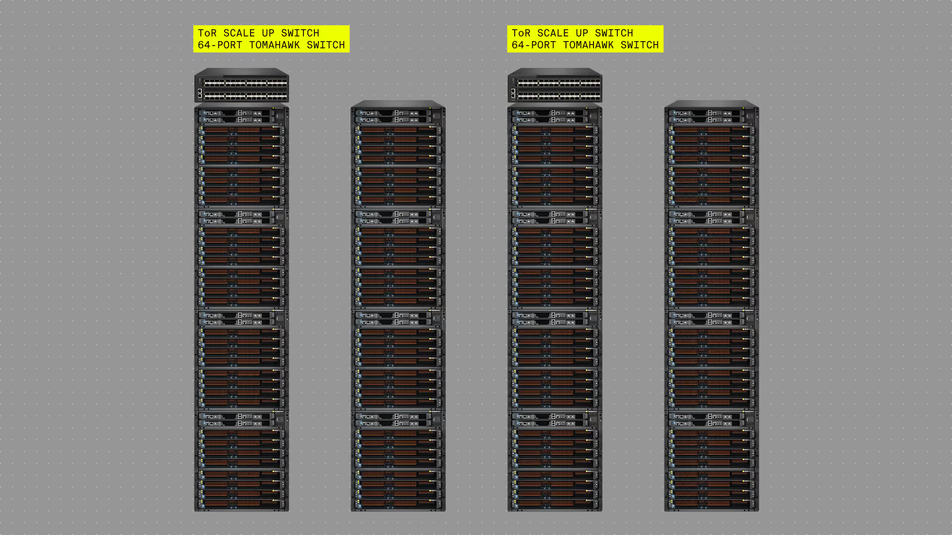
This creates some very interesting possibilities for giant MoEs. With a 1,024-chip Napier Ultra system, a model like Kimi K3 can be deployed in a “native expert” configuration: each of its 896 experts can live on its own AIP. At low batch sizes, that means an AIP will typically need to load only one active expert — dramatically reducing weight-loading time while preserving extremely high per-user speeds.
Multiple 1M Kimi K3 contexts can be re-activated (promote from warm to hot) within <<100ms in parallel. Napier Ultra can hold a total of ~10,000 max-length Kimi K3 contexts and extends the RDMA domain to 140 TB of HBM3e.
Tensordyne Napier: Built from the Math Up
The math is where it starts. The system is where it pays off.
Tensordyne Napier was built from our belief that fast and affordable AI inference starts from the math up. But math alone isn’t enough. Compute, memory, interconnect, and software all have to work together to deliver the most valuable tokens at the least power. One weak link gives the gains back. That is what we set out to fix.
Next Up
We at Tensordyne couldn’t be more excited to bring the first Tokenmaxxer AI inference system to you - and thereby unlock new levels of speed and affordability across all model sizes and modalities. Stay tuned as we release more information in the coming months, leading up to our full product launch.
Reach Out
Contact us at contact@tensordyne.ai for more information or to inquire about early access to Beta systems. Or visit us at https://www.tensordyne.ai/careers if you are inspired to join us.
Endless Thanks
And of course we would like to thank all of our amazing investors and partners who have been instrumental in the development of Tensordyne Napier.
Notes
1 NVIDIA, GTC 2026 Keynote, Jensen Huang, March 2026. Projected Vera Rubin + Groq LPX performance and token economics for GPT-like MoE models up to 2T parameters.
2 SemiAnalysis, OpenAI Jalapeño: Better Than Nvidia Blackwell, August 2026; InferenceX, Output Token Throughput per All-in Utility MW vs. Interactivity, DeepSeek-R1-0528 671B, FP4, 8K/1K, updated August 22, 2026, is the source for the Jalapeño and Vera Rubin data.
3 Napier has taped out and is now in fabrication. Performance is based on modeling and simulation and will be verified upon silicon availability.
4 Elon Musk (xAI), X post, April 2026. States that xAI is training a 10T-parameter model on Colossus 2. https://x.com/elonmusk/status/2041754402239975479
5 Reliable Data Engineering, The Most Powerful AI Ever Built — Claude Mythos (Leaked), Medium, March 2026. Speculates that Claude Mythos has approximately 10-trillion-parameters based on leaked Anthropic draft materials; final specifications had not been officially confirmed.
6 Juniper Networks, Accelerate Grid Modernization with Assured Reliability and Cybersecurity, 2021; Junos OS High Availability User Guide, June 2025; PTX10008 System Overview. HPE Juniper documents 99.999% uptime for core and critical applications, supported by redundant hardware and fault-tolerant high-availability architecture.
7 Financial Times, Nvidia to poach top staff from AI chip start-up Groq in licensing deal, December 2025; Axios, Nvidia deal a big win for Groq employees and investors, December 2025. Axios reported the transaction value at approximately $20B, while Groq remained technically independent under a licensing-and-hiring structure.
8 Nasdaq, Cerebras IPO: Ushering in a New Era of AI Hardware, May 2026. Cerebras priced its IPO at $185 per share, implying a fully diluted valuation of approximately $56.4B.
9 SemiAnalysis, InferenceX, August 2026. Tensordyne MFU calculation based on Blackwell GB300 DeepSeek-R1 performance. https://inferencex.semianalysis.com/inference
10 CoreWeave, NVIDIA Vera Rubin NVL72 on CoreWeave: 10x More Tokens per Megawatt than Blackwell, July 2026. Tensordyne MFU calculation based on Vera Rubin DeepSeek-R1 performance.
11 Bernstein Research, AI datacenter cost analysis, 2025–2026, as reported by Investing.com; MUFG, The AI Weekly: Relative AI Computational Power, February 2026. Bernstein estimates GPUs alone account for approximately 39% of total CapEx for a 1-GW Nvidia-based AI datacenter.
12 Casey Crownhart, In a First, Google Has Released Data on How Much Energy an AI Prompt Uses, MIT Technology Review, August 2025. Google reports that AI accelerator (TPU) compute accounts for roughly 58% of the energy used to serve the median Gemini prompt.
13 Bill Dally (NVIDIA), Logarithmic Numbers and Asynchronous Accumulators: The Future of DL Chips, MLSys 2021; and Trends in Deep Learning Hardware, Paul G. Allen School Distinguished Lecture Series, 2023.
14 Bryon Moyer, Recogni Delivers One Petaop/s, Microprocessor Report, June 2022; Sally Ward-Foxton, Recogni’s 25-W Chip for AVs Processes High-Res Camera Streams, EE Times, January 2024. Recogni is now Tensordyne.
15 Competitor specifications are based on publicly available information and best estimates where necessary.